

AlTiSiN-AlCrSiN nanocrystalline-amorphous multilayer composite superhard toughness coating material and manufacturing method
A multi-layer composite, nanocrystalline technology, applied in coating, metal material coating process, vacuum evaporation plating and other directions, can solve the problems of the influence of coating cutting performance, etc., to improve surface quality, superior temperature resistance and wear resistance. , Overcome the effect of insufficient temperature resistance and wear resistance
- Summary
- Abstract
- Description
- Claims
- Application Information
AI Technical Summary
Problems solved by technology
Method used
Image

Examples
Embodiment 1
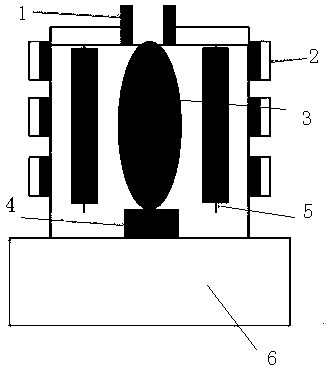
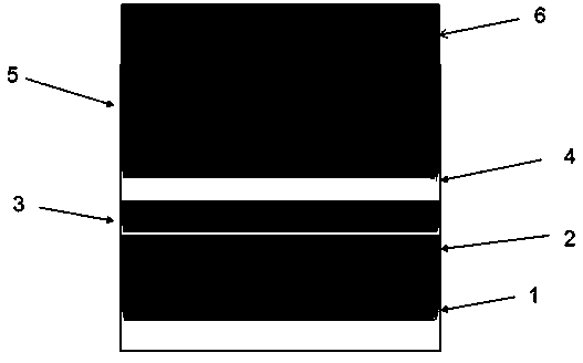
[0042] Example 1: At 100°C and in an argon atmosphere, high-speed steel and hard alloy tools and molds are etched by arc plasma, and then a transition metal with a thickness of 5 nanometers is deposited under the conditions of 0.02-0.2Pa and -800V to -1000V Cr bonding layer; Deposit a 10nm thick CrN layer at 0.1Pa, -20V; deposit a 1500nm AlCrSiN / CrN hardened layer at 0.5Pa pressure, -50V bias; deposit at 0.5 pressure, -50V bias 500nm AlTiSiN / CrN support layer; finally, 0.2 micron AlTiSiN-AlCrSiN multilayer coating is deposited under the condition of 0.5Pa pressure and -20V bias. 3 N 4 The thickness of the amorphous layer is 0.1 nm. The diameter of AlCrN nanocrystals in the AlCrSiN layer is 15 nm, and the Si 3 N 4 The thickness of the amorphous layer is 0.1 nm. The silicon content in the AlTiSiN and AlCrSiN layers is 1 at.%; the total thickness of the coating is 2.205 microns. After the preparation, it is naturally cooled to obtain an AlTiSiN-AlCrSiN nanocrystalline-amorpho...
Embodiment 2
[0043]Embodiment 2: at 450 ℃, under argon atmosphere, high-speed steel and cemented carbide cutting tool and mold are through arc plasma etching, at 0.2Pa, the transition metal Cr binding layer of 200 nanometers is deposited under the condition of -1000V; Deposit a 300nm thick CrN layer at 2.3Pa and -300V; deposit a 200nm AlCrSiN / CrN hardened layer at 8Pa pressure and -300V bias; deposit a 1500nm AlTiSiN / CrN support at 8Pa pressure and -300V bias layer; finally, a 10-micron AlTiSiN-AlCrSiN multilayer coating is deposited under the condition of 10Pa pressure and -300V bias. 3 N 4 The thickness of the amorphous layer is 2 nm. The diameter of AlCrN nanocrystals in the AlCrSiN layer is 5 nm, and the Si 3 N 4 The thickness of the amorphous layer is 2 nm. The silicon content in the AlTiSiN and AlCrSiN layers is 15 at.%; the total thickness of the coating is 12.1 microns. After the preparation is completed, it is cooled naturally to obtain an AlTiSiN-AlCrSiN nanocrystalline-amorp...
Embodiment 3
[0044] Embodiment 3: Under 350 ℃, argon atmosphere, high-speed steel and cemented carbide cutting tool and mold are etched through arc light plasma, at 0.1Pa, the transition metal Cr binding layer of 100 nanometers is deposited under the condition of -800V; Deposit 100nm thick CrN layer under 1.5Pa, -100V condition; deposit 500nm AlCrSiN / CrN hardened layer under 0.5Pa pressure, -100V bias condition; deposit 1000nm AlTiSiN / CrN under 0.5 pressure, -100V bias condition Support layer; finally, 5 micron AlTiSiN-AlCrSiN multi-layer coating is deposited under the condition of 3Pa pressure and -20V bias. The diameter of AlTiN nanocrystal in the AlTiSiN layer in the above coating is 10 nanometers, Si 3 N 4 The thickness of the amorphous layer is 1 nm. The diameter of AlCrN nanocrystals in the AlCrSiN layer is 10 nm, and the Si 3 N 4 The thickness of the amorphous layer is 1 nm. The silicon content in the AlTiSiN and AlCrSiN layers is 5 at.%; the total thickness of the coating is 6....
PUM
| Property | Measurement | Unit |
|---|---|---|
| Diameter | aaaaa | aaaaa |
| Thickness | aaaaa | aaaaa |
| Diameter | aaaaa | aaaaa |
Abstract
Description
Claims
Application Information