

Organic light emission diode device and fabrication method thereof
An electroluminescent device and luminescent technology, which are applied in the manufacture of organic semiconductor devices, electric solid devices, semiconductor/solid state devices, etc., can solve the problems of low device life and low luminous efficiency of organic electroluminescent devices, and achieve strong absorption Electronic properties, high-efficiency injection, and the effect of improving injection efficiency
- Summary
- Abstract
- Description
- Claims
- Application Information
AI Technical Summary
Problems solved by technology
Method used
Image

Examples
Embodiment 1
[0028] A method for preparing an organic electroluminescent device, comprising the following steps:
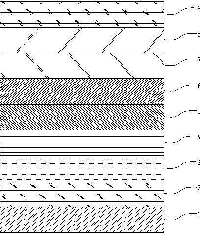
[0029] (1) A glass substrate is provided, and a conductive anode is prepared by vacuum sputtering on the surface of the glass substrate. The conductive anode is indium tin oxide (ITO), and a conductive anode is prepared by vacuum sputtering on the surface of the substrate 1, wherein,
[0030] The pressure when sputtering to prepare conductive anode is 1×10 -3 Pa, accelerating voltage 300V, power density 10W / cm 2 , The sputtering thickness is 70nm.
[0031] (2) The first hole injection auxiliary layer is vacuum evaporated on the surface of the conductive anode, and the material of the first hole injection auxiliary layer is molybdenum trioxide (MoO 3 ), the pressure when the first hole injection auxiliary layer is evaporated is 1×10 -3 Pa, the evaporation rate is 0.1nm / s, and the evaporation thickness is 0.5nm.
[0032] (3) The second hole injection auxiliary layer is vac...
Embodiment 2
[0043] A method for preparing an organic electroluminescent device, comprising the following steps:
[0044] (1) A glass substrate is provided, and a conductive anode is prepared by vacuum sputtering on the surface of the glass substrate. The conductive anode is made of indium zinc oxide (IZO), and a conductive anode is prepared by vacuum sputtering on the surface of the substrate. Among them,
[0045] The pressure when sputtering to prepare conductive anode is 1×10 -5 Pa, acceleration voltage is 800V, power density is 40W / cm 2 , the sputtering thickness is 200nm.
[0046] (2) The first hole injection auxiliary layer is vacuum evaporated on the surface of the conductive anode, and the material of the first hole injection auxiliary layer is vanadium pentoxide (V 2 o 5 ), the pressure when the first hole injection auxiliary layer is evaporated is 1×10 -5 Pa, the evaporation rate is 1nm / s, and the evaporation thickness is 5nm.
[0047] (3) The second hole injection auxiliary...
Embodiment 3
[0058] A method for preparing an organic electroluminescent device, comprising the following steps:
[0059] (1) A glass substrate is provided, and a conductive anode is prepared by vacuum sputtering on the surface of the glass substrate. The conductive anode is aluminum zinc oxide (AZO), and a conductive anode is prepared by vacuum sputtering on the surface of the substrate. Among them,
[0060] The pressure when sputtering to prepare conductive anode is 1×10 -4 Pa, accelerating voltage is 600V, power density is 20W / cm 2 , the sputtering thickness is 100nm.
[0061] (2) The first hole injection auxiliary layer is vacuum evaporated on the surface of the conductive anode, and the material of the first hole injection auxiliary layer is tungsten trioxide (WO 3 ), the pressure when the first hole injection auxiliary layer is evaporated is 1×10 -4 Pa, the evaporation rate is 0.1nm / s, and the evaporation thickness is 2nm.
[0062] (3) The second hole injection auxiliary layer is...
PUM
| Property | Measurement | Unit |
|---|---|---|
| Thickness | aaaaa | aaaaa |
| Thickness | aaaaa | aaaaa |
| Thickness | aaaaa | aaaaa |
Abstract
Description
Claims
Application Information