

Organic electroluminescent device
An electroluminescent device and electroluminescent technology, which can be applied in the direction of electro-solid devices, electrical components, semiconductor devices, etc., and can solve the problems of high voltage, low brightness, low efficiency, etc.
- Summary
- Abstract
- Description
- Claims
- Application Information
AI Technical Summary
Problems solved by technology
Method used
Image

Examples
Embodiment 1
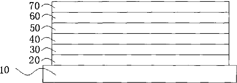
[0026] figure 1 It is a cross-sectional view of the structure of the organic electroluminescent device in this embodiment, including a substrate 10 , an anode layer 20 , a hole transport layer 30 , a light emitting layer 40 , a first cathode layer 50 , a second cathode layer 60 and a third cathode layer 70 . The device structure of the organic electroluminescent device in this embodiment is as follows:
[0027] Glass substrate / ITO / NPB(50nm) / Alq 3 (50nm) / Li 3 N(1nm) / Mg:Ag(100nm, 10%) / Ag(80nm)
[0028] Preparation steps:
[0029] (1) Preparation of organic light-emitting layer
[0030] An ITO (indium tin oxide) film is prepared on the glass substrate as an anode, the sheet resistance of the ITO film is 50Ω, and the film thickness is 150 nm. Place the glass substrate with the prepared anode in the vacuum chamber and evacuate to 1×10 -3 Pa, the hole transport material NPB is evaporated, the evaporation rate of the material film is 0.1nm / s, and the film thickness is 50nm; on ...
Embodiment 2
[0037] The structural cross-sectional view of the organic electroluminescent device in this embodiment is as follows figure 1 As shown, the substrate 10 , the anode layer 20 , the hole transport layer 30 , the light emitting layer 40 , the first cathode layer 50 , the second cathode layer 60 and the third cathode layer 70 . The device structure of the organic electroluminescent device in the embodiment of the present invention is as follows:
[0038] Glass substrate / ITO / NPB(50nm) / Alq 3 (50nm) / CsCO 3 (2nm) / Mg:Al(300nm, 20%) / Al(50nm)
[0039] Preparation steps:
[0040] (1) Preparation of the organic light-emitting layer: same as the preparation step (1) of Example 1.
[0041] (2) Preparation of cathode layer
[0042] Evaporate 2nm CsCO on the emitting layer 3 As the first cathode layer of the device, its evaporation rate is 0.05nm / s;
[0043] After the first cathode layer was prepared, the second cathode layer was prepared by vapor deposition, and the mixture of Mg and A...
Embodiment 3
[0047] The structural cross-sectional view of the organic electroluminescent device in this embodiment is as follows figure 1 As shown, the substrate 10 , the anode layer 20 , the hole transport layer 30 , the light emitting layer 40 , the first cathode layer 50 , the second cathode layer 60 and the third cathode layer 70 . The device structure of the organic electroluminescent device in the embodiment of the present invention is as follows:
[0048] Glass substrate / ITO / NPB(50nm) / Alq 3 (50nm) / KBH 4 (0.5nm) / Mg:Ag(50nm, 5%) / Ag(150nm)
[0049] Preparation steps:
[0050] (1) Preparation of the organic light-emitting layer: same as the preparation step (1) of Example 1.
[0051] (2) Preparation of cathode layer
[0052] Evaporate 0.5nm KBH on the light-emitting layer 4 As the first cathode layer of the device, its evaporation rate is 0.05nm / s;
[0053] After the first cathode layer was prepared, the second cathode layer was prepared by vapor deposition, and the mixture of M...
PUM
| Property | Measurement | Unit |
|---|---|---|
| Thickness | aaaaa | aaaaa |
| Thickness | aaaaa | aaaaa |
| Thickness | aaaaa | aaaaa |
Abstract
Description
Claims
Application Information