

Production of low-density carbon nanotube array composite electrode and application of same and in glucose sensor
A carbon nanotube array and composite electrode technology, which is applied in the direction of instruments, scientific instruments, and electrochemical variables of materials, to achieve the effects of wide detection linear range, high sensitivity, and low response
- Summary
- Abstract
- Description
- Claims
- Application Information
AI Technical Summary
Problems solved by technology
Method used
Image

Examples
Embodiment 1
[0068] Composite electrodes were prepared using the following steps:
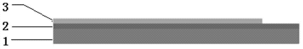
[0069] 1. Select the surface with SiO 2 Oxide layer of silicon wafer as the substrate, where SiO 2 Layer as an insulating layer, its thickness is between 100-200nm.
[0070] 2. Cut the silicon wafer into 25×3mm rectangular test pieces, ultrasonically clean them with acetone, isopropanol (IPA) and deionized water for 5-8 minutes respectively, and then dry them with a nitrogen gun for later use.
[0071] 3. Place the rectangular test piece in the magnetron sputtering chamber, cover the working area with PTFE vacuum tape and aluminum foil, set the sputtering power to 50-100W, and the working pressure to 3.5×10 -3 mbar, the target material is a tungsten target with a purity of 99.99%, and the sputtering gas is high-purity argon. The thickness of tungsten as the conductive layer is between 30-60nm.
[0072] 4. Place high-purity ITO and nickel targets in a multi-target magnetron sputtering apparatus, and cove...
Embodiment 2
[0077] Composite electrodes were prepared using the following steps:
[0078] 1. repeat the 1-4 steps in the embodiment (1)
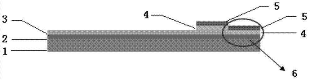
[0079] 2. Sputter a layer of Ni film on the basis of the ITO film. The thickness of the Ni layer has an important influence on the growth and density of the CNT array. When the thickness is 8nm, the CNT array density is 10 8 -10 9 / cm 2 .
[0080] 3. Repeat the 6th step in embodiment (1)
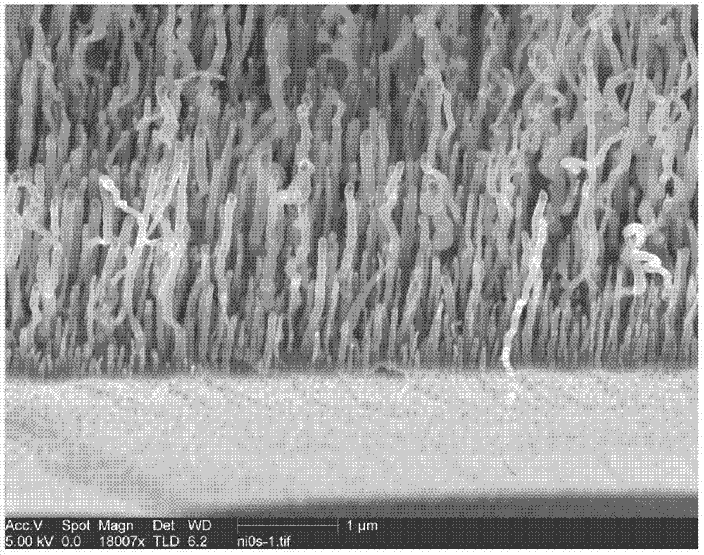
[0081] 4. Place the CNT array sample in magnetron sputtering, using a high-purity Ni target, set the sputtering power to 50-100W, and the working pressure to 3.5×10 -3 mbar, the sputtering gas is high-purity argon, the sputtering time is 180 seconds, and the diameter of the nano-Ni particles is about 4nm (see attached image 3 ). In order to obtain nanoscale Ni particles, the deposition rate of Ni is as slow as
Embodiment 3
[0083] Composite electrodes were prepared using the following steps:
[0084] 1. repeat the 1-4 steps in the embodiment (1)
[0085] 2. Sputter a layer of Ni film on the basis of the ITO film. The thickness of the Ni layer has an important influence on the growth and density of the CNT array. When the thickness is 15nm, the CNT array density is 10 9 -10 10 / cm 2 .
[0086] 3. Repeat the 6th step in embodiment (1)
[0087] 4. Place the CNT array sample in magnetron sputtering, using a high-purity Ni-Fe alloy target, set the sputtering power to 50-100W, and the working pressure to 3.5×10 -3 mbar, the sputtering gas is high-purity argon, the sputtering time is 360 seconds, and the diameter of nano-Ni-Fe composite particles is about 9 nm.
PUM
| Property | Measurement | Unit |
|---|---|---|
| height | aaaaa | aaaaa |
| thickness | aaaaa | aaaaa |
| thickness | aaaaa | aaaaa |
Abstract
Description
Claims
Application Information