

Transparent conductive film and preparation method thereof
A technology of a transparent conductive film and a transparent substrate, applied in the field of electronics, can solve the problems of uneven conduction of metal nanowire films and easy changes in electrical conductivity, and achieve the effects of high stability, weakened oxidation, and good conduction uniformity.
- Summary
- Abstract
- Description
- Claims
- Application Information
AI Technical Summary
Problems solved by technology
Method used
Image

Examples
Embodiment 1
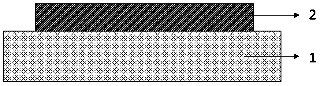
[0037] Complete the preparation of the transparent conductive film 2 through the following specific steps:
[0038] 1) Cleaning the glass substrate 1 with deionized water, acetone solution and isopropanol, drying it with dry nitrogen after cleaning, and treating the substrate surface with oxygen plasma or ultraviolet light / ozone;
[0039] 2) preparing a silver nanowire dispersion, the silver nanowire has a diameter of 40nm and a length of 200 μm, the solvent in the silver nanowire dispersion is ethanol, and the concentration of the silver nanowire in the solvent is 3mg / ml;
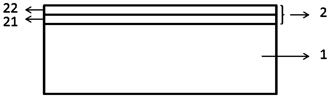
[0040] 3) forming a silver nanowire layer 21 on the transparent substrate 1 by spin coating;
[0041] 4) Form a conductive polymer layer 22 on the silver nanowire layer 21 by spin coating, and the conductive polymer is PEDOT:PSS with a neutral pH value;
[0042] 5) Transfer the transparent substrate 1 containing the silver nanowire layer 21 and the conductive polymer layer 22 to a heating table, and dry t...
Embodiment 2
[0044] Complete the preparation of the transparent conductive film 2 through the following specific steps:
[0045]1) Clean the polyethylene terephthalate (PET) flexible transparent substrate 1 with deionized water, acetone solution and isopropanol, blow it dry with dry nitrogen after cleaning, and use oxygen plasma or ultraviolet light / Ozone treatment of the substrate surface;
[0046] 2) preparing a copper nanowire dispersion, the copper nanowire has a diameter of 100 nm and a length of 100 μm, the solvent in the copper nanowire dispersion is methanol, and the concentration of the copper nanowire in the solvent is 2 mg / ml;
[0047] 3) forming a copper nanowire layer 21 on the transparent substrate 1 by scraping;
[0048] 4) Form a conductive polymer layer 22 on the copper nanowire layer 21 by spin coating, and the conductive polymer is PEDOT:PSS with a neutral pH value;
[0049] 5) Transfer the transparent substrate 1 containing the copper nanowire layer 21 and the condu...
Embodiment 3
[0051] Complete the preparation of the transparent conductive film 2 through the following specific steps:
[0052] 1) Clean the polyethylene naphthalate (PEN) flexible transparent substrate 1 with deionized water, acetone solution and isopropanol, blow it dry with dry nitrogen after cleaning, and use oxygen plasma or ultraviolet light / Ozone treatment of the substrate surface;
[0053] 2) Prepare copper nanowire dispersion, the diameter of the copper nanowire is 200nm, the length is 30 μm, the solvent in the copper nanowire dispersion is methanol, and the concentration of the copper nanowire in the solvent is 0.1mg / ml ;
[0054] 3) Forming a copper nanowire layer 21 on the transparent substrate 1 by spraying;
[0055] 4) A conductive polymer layer 22 is formed on the copper nanowire layer 21 by scraping, and the conductive polymer is PEDOT:PSS with a neutral pH value;
[0056] 5) Transfer the transparent substrate 1 containing the copper nanowire layer 21 and the conductiv...
PUM
| Property | Measurement | Unit |
|---|---|---|
| Length | aaaaa | aaaaa |
| Diameter | aaaaa | aaaaa |
| Diameter | aaaaa | aaaaa |
Abstract
Description
Claims
Application Information