Field effect diode and manufacturing method thereof

A field-effect diode and anode technology, which is applied in the direction of diode, semiconductor/solid-state device manufacturing, electrical components, etc., can solve the problem of increasing reverse leakage current of Schottky diode, degradation of electrical performance of Schottky diode, increase of on-state loss, etc. problem, to achieve the effect of good crystal quality, lower forward voltage drop, and lower forward conduction resistance

Active Publication Date: 2014-12-24
GPOWER SEMICON
View PDF4 Cites 18 Cited by
  • Summary
  • Abstract
  • Description
  • Claims
  • Application Information

AI Technical Summary

Problems solved by technology

But this also increases the reverse leakage current of the Schottky diode
Moreover, the lower barrier height will degrade the electrical performance of the Schottky diode at high temperature, such as th

Method used


Image

  • Field effect diode and manufacturing method thereof
  • Field effect diode and manufacturing method thereof
  • Field effect diode and manufacturing method thereof

Examples


Embodiment Construction

[0061] The present invention will be described in detail below in conjunction with specific embodiments shown in the accompanying drawings. However, these embodiments do not limit the present invention, and any structural, method, or functional changes made by those skilled in the art according to these embodiments are included in the protection scope of the present invention.

[0062] Furthermore, repeated reference numerals or designations may be used in different embodiments. These repetitions are merely for the sake of simplicity and clarity of describing the present invention, and do not imply any relationship between the different embodiments or structures discussed.

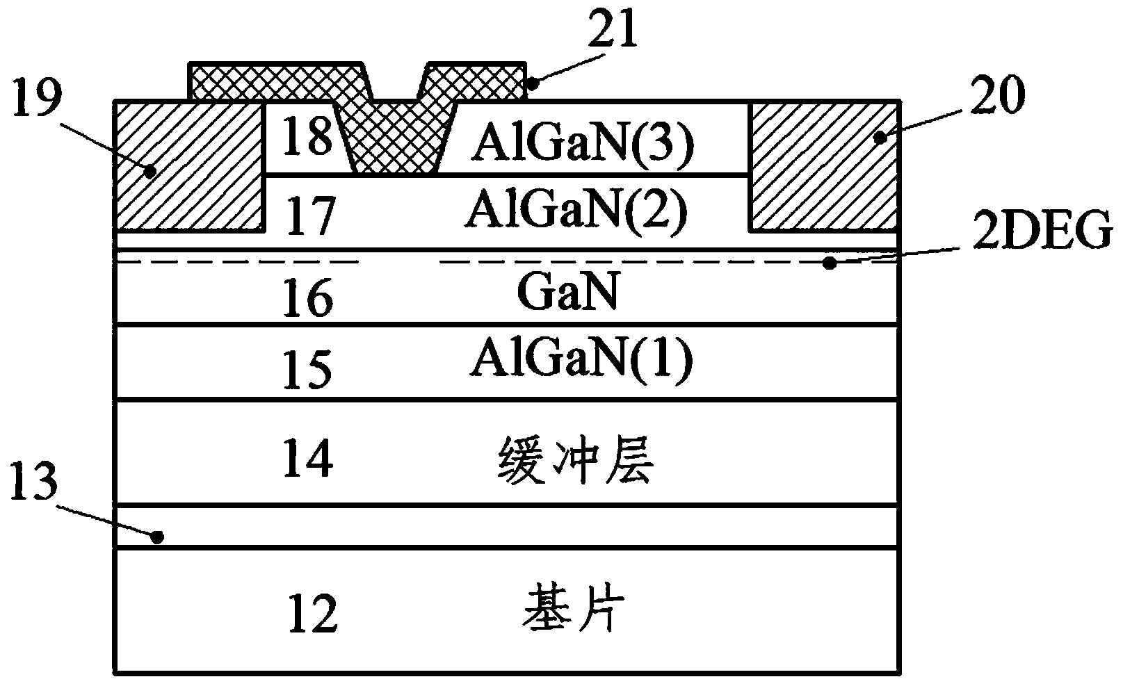
[0063] The invention discloses a field effect diode, comprising:

[0064] Substrate;

[0065] a nucleation layer on said substrate;

[0066] a buffer layer located on the nucleation layer;

[0067] a back barrier layer on the buffer layer;

[0068] a channel layer on the back barrier layer;

[0069] ...


PUM

PropertyMeasurementUnit
Thicknessaaaaaaaaaa
Thicknessaaaaaaaaaa
Thicknessaaaaaaaaaa

Abstract

The invention discloses a field effect diode and a manufacturing method of the field effect diode. The field effect diode sequentially comprises a substrate, a nucleating layer, a buffering layer, a back barrier layer, a channel layer, a first barrier layer and a second barrier layer. A groove, an anode and a cathode are arranged on the second barrier layer. The cathode is an ohmic contact electrode. The anode is of a composite structure and is composed of the ohmic contact electrode and a schottky electrode which is located in the groove and is connected with the ohmic contact electrode in a short circuit mode. The first barrier layer and the back barrier layer have similar constituent content, the second barrier layer is different from the first barrier layer in constituent content, and the lattice constant of the second barrier is smaller than that of the first barrier layer. The field effect diode has smaller positive conductive voltage drop, smaller reverse leakage current and larger breakdown voltage.

Description

technical field [0001] The invention relates to the technical field of semiconductors, in particular to a field effect diode based on energy band engineering, low forward conduction voltage drop, low reverse leakage current and high breakdown voltage and a manufacturing method thereof. Background technique [0002] In modern society, power electronics technology in many fields, such as high-voltage power supply, power conversion, factory automation, and motor vehicle energy distribution management, continues to develop. Power semiconductor devices are usually used as switches or rectifiers in circuit systems and are an important part of power electronics technology. Power devices determine the consumption and efficiency of the circuit system, and play a very important role in energy saving and consumption reduction. In recent years, GaN Schottky diodes with high frequency, high power density, and low power consumption have aroused great interest in the industry due to their...

Claims


Application Information

Patent Timeline
IPC IPC(8): H01L29/872H01L29/06H01L21/329
CPCH01L29/475H01L29/66462H01L29/7789H01L29/402H01L29/66212H01L29/7783H01L29/2003H01L29/205H01L29/872H01L29/66143
Inventor 陈洪维
Owner GPOWER SEMICON
Why Eureka
Try Eureka