An electrostatic discharge protection structure

An electrostatic discharge protection and isolation structure technology, applied in circuits, electrical components, electrical solid devices, etc., can solve problems such as high breakdown voltage, inability to protect chips or semiconductor devices from electrostatic damage, and reduced chip energy consumption, and achieve heat dissipation capabilities. Good, the effect of eliminating heat accumulation and avoiding burning

Active Publication Date: 2014-12-31
SEMICON MFG INT (SHANGHAI) CORP
View PDF5 Cites 6 Cited by
  • Summary
  • Abstract
  • Description
  • Claims
  • Application Information

AI Technical Summary

Problems solved by technology

[0005] However, with the development of semiconductor technology, the size of semiconductor devices continues to shrink, so that the energy consumption of the chip is continuously reduced, and its operating voltage is continu

Method used


Image

  • An electrostatic discharge protection structure
  • An electrostatic discharge protection structure
  • An electrostatic discharge protection structure

Examples


Embodiment Construction

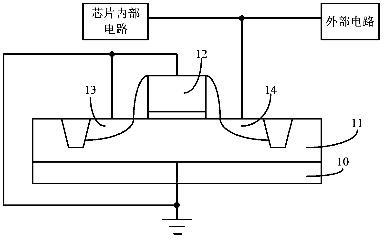
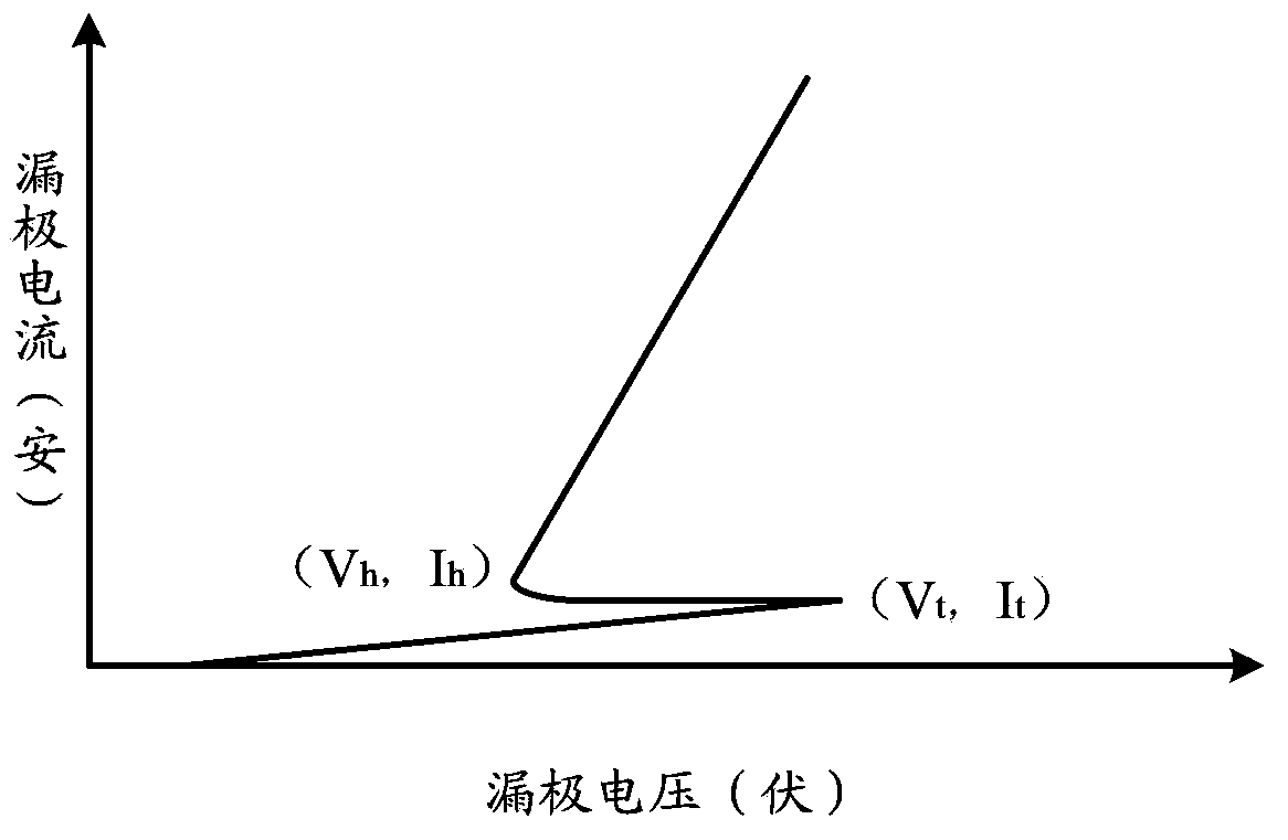
[0028] As mentioned in the background art, the breakdown voltage of the existing electrostatic discharge protection structure is too high to meet the technical requirements for protecting low-voltage chips or devices.

[0029] Existing grounded N-type field effect transistor breakdown voltage V t Typically 5.8V. As the size of a chip or semiconductor device decreases, its operating voltage also decreases accordingly, and the voltage that can cause damage to the chip or semiconductor device also decreases accordingly. Taking the transistor whose operating voltage is reduced to 1.2V as an example, please refer to Figure 8 , is the I / V characteristic diagram of the gate current and gate voltage of the transistor with the operating voltage of 1.2V. Due to the reduction in the size of the transistor, the thickness of the gate oxide layer in the transistor is also reduced accordingly, resulting in The breakdown voltage of the gate oxide V b(breakdown voltage) is reduced to 5.9V....


PUM


Abstract

The invention discloses an electrostatic discharge protection structure, which comprises a well region within a substrate, wherein the well region has doping ions of a first conductivity type therein and is electrically connected with a ground terminal; a second doped region within the substrate, wherein the second doped region is located on the surface of the well region, and has doping ions of a second conductivity type therein, wherein a doping concentration in the second doped region is higher than that in the well region; a first doped region within the substrate, wherein the first doped region is located on the surface of the second doped region, and a surface of the first doped region is flush with the substrate surface, wherein the first doped region has doping ions of a first conductivity type therein and is electrically connected with an electrostatic discharge input terminal, and wherein a doping concentration in the first doped region is higher than that in the second doped region, and the doping concentration difference between the first doped region and the second doped region is smaller than that between the second doped region and the well region. The electrostatic discharge protection structure has a low breakdown voltage so as to be improved in a protective capability.

Description

technical field [0001] The invention relates to the technical field of semiconductor manufacturing, in particular to an electrostatic discharge protection structure. Background technique [0002] As semiconductor chips are used more and more widely, there are more and more factors that cause semiconductor chips to be damaged by static electricity. In existing chip designs, electrostatic discharge (ESD, Electrostatic Discharge) protection circuits are often used to reduce chip damage. The design and application of existing ESD protection circuits include: Gate Grounded NMOS (GGNMOS) protection circuits, Silicon Controlled Rectifier (SCR) protection circuits, lateral diffusion field effect transistors ( Laterally Diffused MOS, LDMOS) protection circuit, etc. [0003] figure 1 It is a schematic cross-sectional structure diagram of an existing gate-grounded N-type field effect transistor protection structure, including: a substrate 10; a P-type well region 11 located in the s...

Claims


Application Information

Patent Timeline
IPC IPC(8): H01L27/02
Inventor 霍晓张莉菲甘正浩代萌俞少峰严北平
Owner SEMICON MFG INT (SHANGHAI) CORP
Why Eureka
Try Eureka