SOI voltage resistance structure with charge regions fixed at equal intervals and SOI power device

A voltage-resistant structure and fixed charge technology, applied in electrical components, semiconductor devices, circuits, etc., can solve the problems of difficult structural design of thin silicon layer SOI devices, serious lateral and vertical expansion of silicon layer charge islands, etc., to alleviate the self-heating effect. , Improve the longitudinal withstand voltage and enhance the effect of electric field strength

Active Publication Date: 2015-01-07
GUILIN UNIV OF ELECTRONIC TECH
View PDF8 Cites 6 Cited by
  • Summary
  • Abstract
  • Description
  • Claims
  • Application Information

AI Technical Summary

Problems solved by technology

Although these interfacial holes can effectively increase the electric field of the dielectric buried layer and improve the withstand voltage, the structure is greatly affected by the subsequent manufacturin

Method used


Image

  • SOI voltage resistance structure with charge regions fixed at equal intervals and SOI power device
  • SOI voltage resistance structure with charge regions fixed at equal intervals and SOI power device
  • SOI voltage resistance structure with charge regions fixed at equal intervals and SOI power device

Examples


Embodiment 1

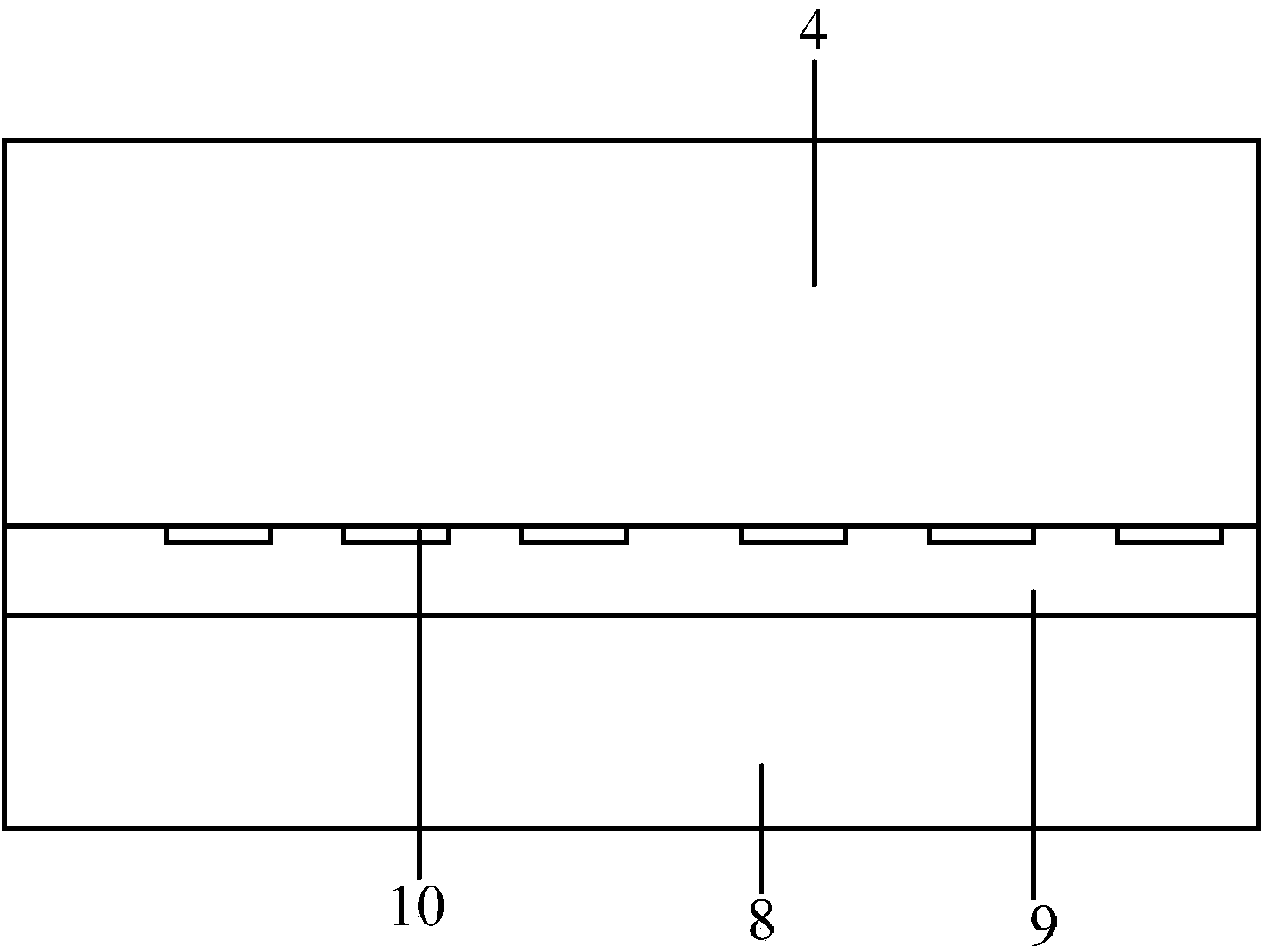
[0034] An equidistant fixed charge island SOI withstand voltage structure, such as figure 2 As shown, the withstand voltage structure at least includes a substrate layer 8, a buried dielectric layer 9 and an active layer 4, and the substrate layer 8, buried dielectric layer 9 and active layer 4 are stacked in sequence from bottom to top. The structures of the substrate layer 8 , the dielectric buried layer 9 and the active layer 4 are the same as or similar to the basic structures of existing power devices in the prior art. The material of the active layer 4 can be Si, SiC, GaAs, SiGe, GaN or other semiconductor materials. The material of the buried dielectric layer 9 may be SiO2 or a low-k material, wherein the low-k material (low dielectric constant) may be carbon-doped oxide or SiOF. However, the material of the active layer 4 and the material of the buried dielectric layer 9 are not limited to the materials listed above. The above-mentioned buried dielectric layer 9 can...

Embodiment 2

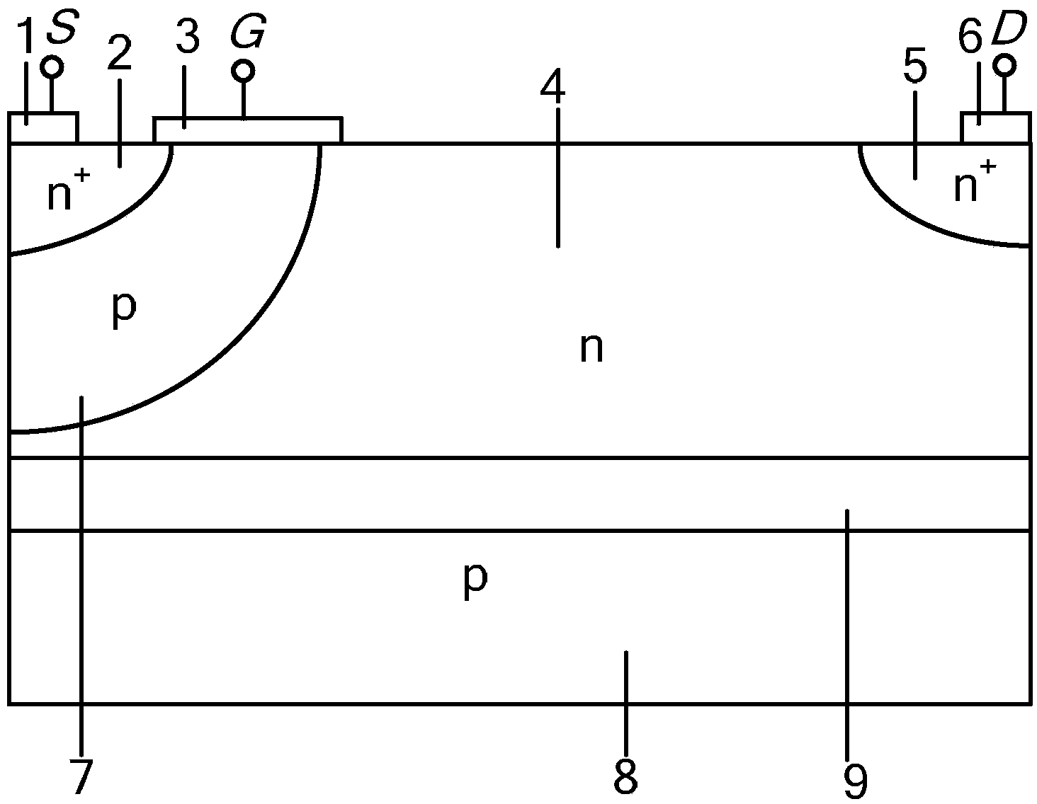
[0039] An SOI power device with equidistant fixed charge island SOI withstand voltage structure, that is, SOI LDMOS device, such as Figure 4 As shown, it includes a substrate layer 8, a dielectric buried layer 9 and an active layer 4 stacked sequentially from bottom to top. An active region 2 , a channel region 7 and a drain region 5 are arranged at upper corners on both sides of the active layer 4 . The source region 2 and the channel region 7 are adjacent to each other, and are arranged at the upper corner of one side of the active layer 4 at the same time. The drain region 5 is disposed at the upper corner of the other side of the active layer 4 . The surface of the active layer 4 is provided with a source 1 , a gate 3 and a drain 6 . The source electrode 1 overlies the source region 2 , and the gate 3 overlies both the source region 2 and the channel region 7 . The drain 6 overlies the drain region 5 . The buried dielectric layer is further provided with a plurality o...

Embodiment 3

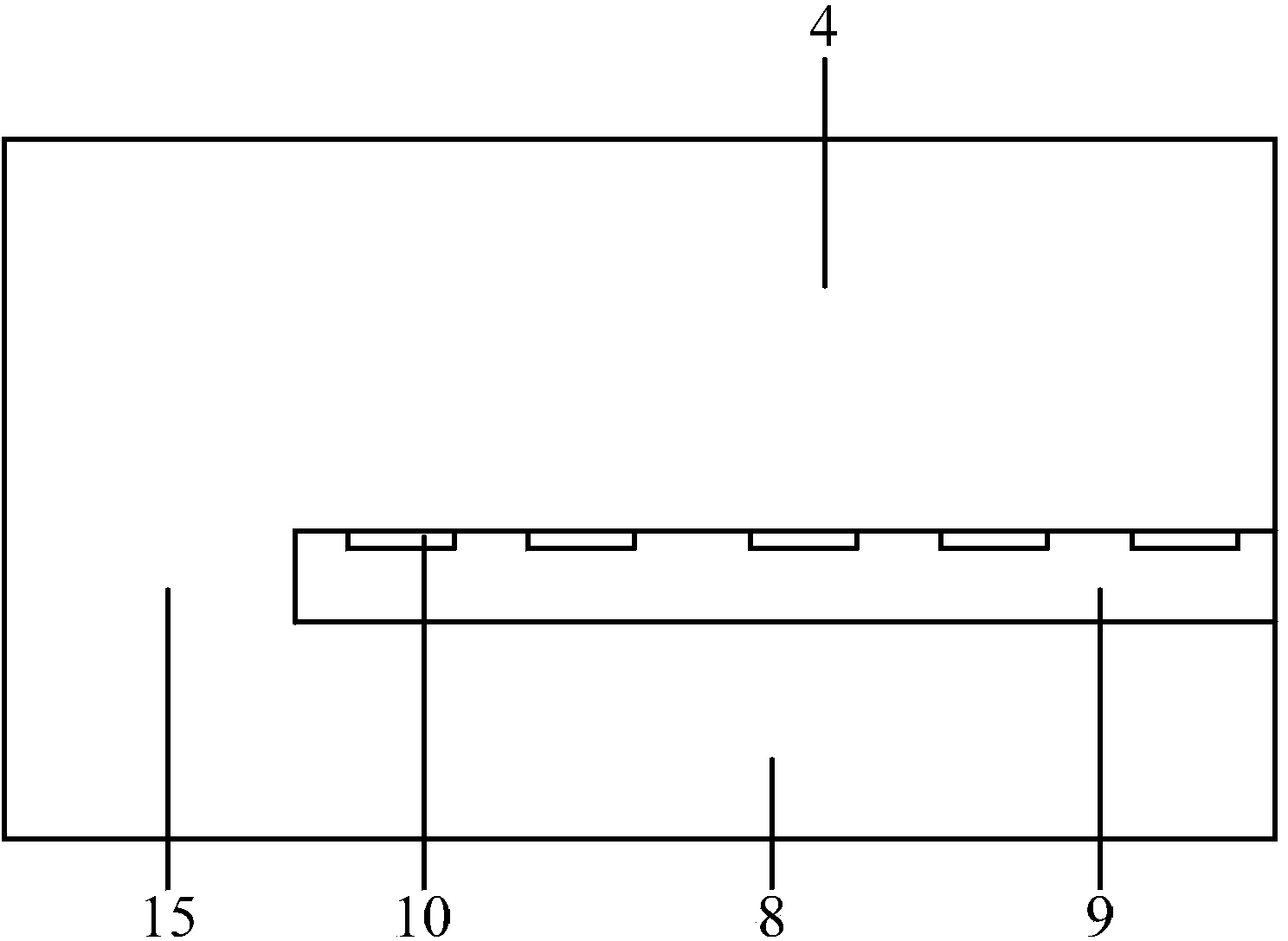
[0043] Another SOI power device with equidistant fixed charge island SOI withstand voltage structure, that is, SOI IGBT device, such as Figure 7 As shown, it includes a substrate layer 8, a dielectric buried layer 9 and an active layer 4 stacked sequentially from bottom to top. A cathode charge region 12 , a channel region 7 and an anode charge region 13 are provided at upper corners on both sides of the active layer 4 . The cathode charge region 12 is in contact with the channel region 7 and is also arranged at the upper corner of one side of the active layer 4 . The anode charge region 13 is disposed at the upper corner of the other side of the active layer 4 . The surface of the active layer 4 is provided with a cathode 11 , a grid 3 and an anode 14 . The cathode 11 overlies the cathode charge region 12 , and the gate 3 overlies both the cathode charge region 12 and the channel region 7 . The anode 14 overlies the anode charge region 13 . The buried dielectric layer is...


PUM


Abstract

The invention discloses an SOI voltage resistance structure with charge regions fixed at equal intervals and a power device. The SOI voltage resistance structure comprises a substrate layer, a dielectric buried layer, an active layer and a plurality of high-concentration fixed charge regions with the concentration larger than or equal to 1*10<13> cm<-2>, wherein the substrate layer, the dielectric buried layer, the active layer and the high-concentration fixed charge regions are stacked in sequence from top to bottom. The high-concentration fixed charge regions are made of a dielectric material, and the charge polarity is positive. The high-concentration fixed charge regions are all located on the dielectric buried layer, arranged in a spaced mode and distributed at equal intervals. According to the SOI voltage resistance structure with the charge regions fixed at equal intervals and the power device, the electric field of the dielectric buried layer can be greatly enhanced, and the voltage resistance capacity is effectively improved; a technology is easy to implement, and is completely compatible with a common CMOS technology.

Description

technical field [0001] The invention belongs to the field of semiconductor power devices, and in particular relates to an SOI voltage-resistant structure with equidistant fixed charge regions and an SOI power device. Background technique [0002] SOI (Silicon On Insulator, silicon on insulating substrate) power devices have high operating speed and integration, reliable insulation performance, strong radiation resistance and no SCR self-locking effect, and are widely used in power electronics, Industrial automation, aerospace and weaponry and other fields. [0003] The breakdown voltage of the SOI power device is calculated by the ionization integration of the electric field along the withstand voltage length, and depends on the smaller of the longitudinal withstand voltage and the lateral withstand voltage. The design principle of SOI lateral withstand voltage can follow the mature silicon-based principles and technologies, such as RESURF (Reduce SURface electric Field, re...

Claims


Application Information

Patent Timeline
IPC IPC(8): H01L29/78H01L29/06
CPCH01L29/7824H01L29/408H01L29/7816H01L29/0603H01L29/7393
Inventor 李琦李海鸥翟江辉唐宁蒋行国李跃
Owner GUILIN UNIV OF ELECTRONIC TECH
Why Eureka
Try Eureka