Methods for making silicon containing films on thin film transistor devices

A silicon-containing film and device technology, applied in transistors, semiconductor/solid-state device manufacturing, semiconductor devices, etc.

Active Publication Date: 2015-01-14
VERSUM MATERIALS US LLC
View PDF8 Cites 9 Cited by
  • Summary
  • Abstract
  • Description
  • Claims
  • Application Information

AI Technical Summary

Problems solved by technology

The above references illustrate that it is challenging to obtain high quality films at lower deposition temperatures

Method used


Image

  • Methods for making silicon containing films on thin film transistor devices
  • Methods for making silicon containing films on thin film transistor devices
  • Methods for making silicon containing films on thin film transistor devices

Examples


Embodiment 1

[0097] Example 1: Deposition of diethylsilane (2ES) and triethylsilane (3ES) at deposition temperatures of 200°C, 250°C, 300°C, 350°C and 400°C

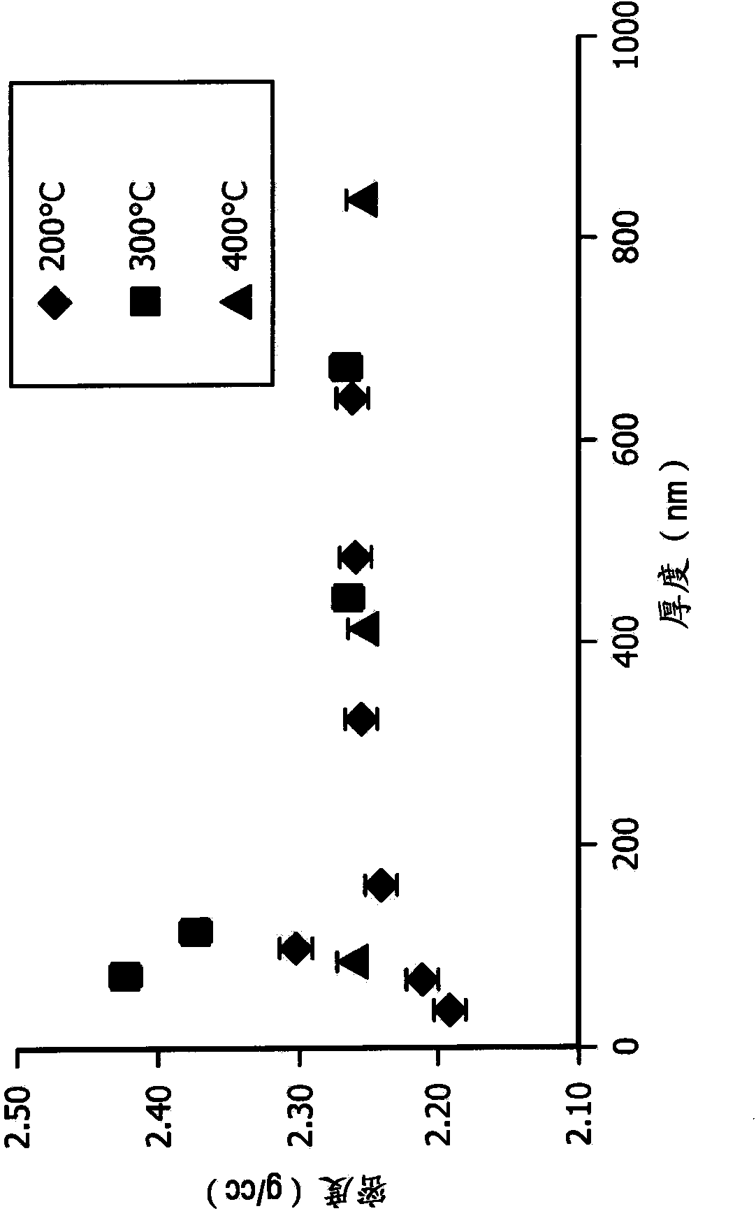
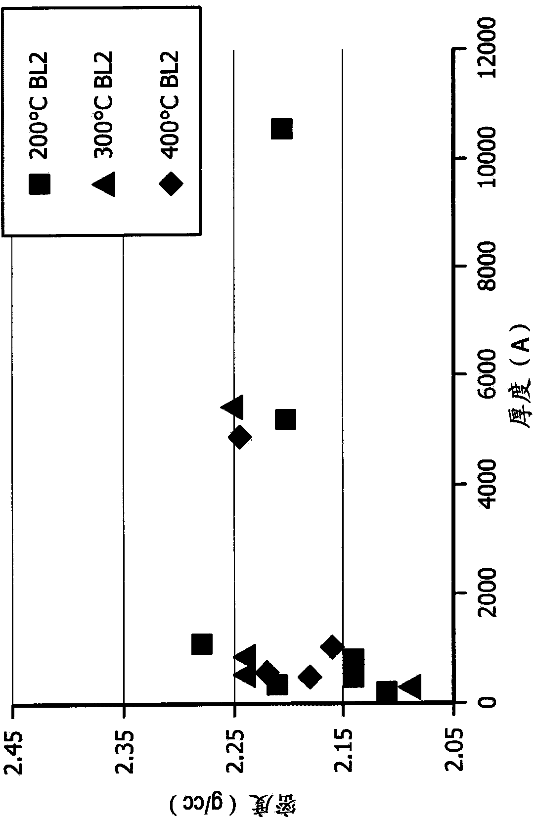
[0098] Silicon oxide films were deposited from silicon precursors 2ES and 3ES. SiO was deposited at different temperatures and process conditions using the general deposition conditions described above 2 membrane. BL-1 and BL-2 conditions were the same except for the precursor flow rate. Although the BL-1 process has the highest deposition rate due to the higher precursor flow rate, for the gate insulating layer, the deposition rate is not the most important criterion. BL-3 is a lower pressure condition and generally gives a poorer membrane. A comparison of the same Si-feed amount between the precursors was used to see if a truly better quality film could be produced. Such as Figure 1A and 2A As seen in , for >200nm films using the BL-2 process, generally higher densities (>2.2g / cc) are obtained, and as Figure 1B , 2B As se...

Embodiment 2

[0104] Example 2: Comparison of silicon oxide films deposited using BL2 process conditions and tetraethoxysilane (TEOS) versus diethylsilane (2ES)

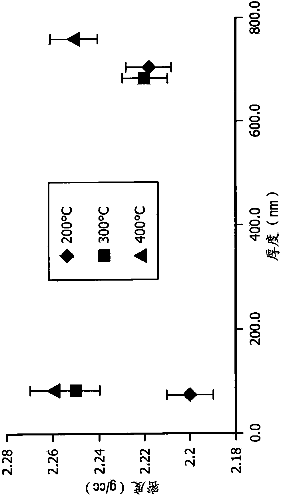
[0105] Deposit SiO using the process conditions described in General Deposition Conditions above and in Table 1 2 membrane. exist Figure 1C and 1D TEOS-deposited silicon oxide films with different thicknesses were deposited under the same BL-2 and BL-3 process conditions described in Table 1 above. refer to Figure 1C , compared with 2ES and 3ES films deposited at the same deposition temperature using BL-2 (see Figure 1A and Figure 2A ) at lower deposition temperatures such as 200 °C, TEOS-deposited films generally have lower densities than 2ES or 3ES films. For the same deposition temperature, comparing Figure 1D The data in and the data of 2ES film and 3ES film ( Figure 1B and 2B A similar effect was observed for . 2ES and 3ES films typically exhibit the same or higher densities for thinner films. In general, the...

Embodiment 3

[0112] Example 3: Deposition of thin SiO with high density using 3ES 2 Membrane and Electrical Properties

[0113] Process conditions for 3ES silicon oxide films were screened using the Design of Experiments (DOE) approach summarized below: precursor flow rate 10 to 200 sccm; O 2 / He flow rate 100 to 1000 sccm, pressure 0.75 to 10 Torr; low frequency (LF) power 0 to 100W; deposition temperature range 25 to 350°C. DOE experiments were used to determine what process parameters yield optimal films for use as gate insulating layers in display devices.

[0114] SiO was deposited using precursor 3ES at even lower deposition temperatures such as 100°C, 125°C and 150°C than those described in the previous examples above 2 membrane. High density and thin SiO obtained by optimizing process parameters such as precursor flow rate, chamber pressure and power density 2 membrane. Table 2 shows the three process conditions for 3ES films deposited at different temperatures: 100°C, 125°C a...


PUM

PropertyMeasurementUnit
thicknessaaaaaaaaaa
thicknessaaaaaaaaaa
densityaaaaaaaaaa

Abstract

Described herein are low temperature processed high quality silicon containing films. Also disclosed are methods of forming silicon containing films at low temperatures. In one aspect, there are provided silicon-containing film having a thickness of about 2 nm to about 200 nm and a density of about 2.2 g / cm3 or greater wherein the silicon-containing thin film is deposited by a deposition process selected from a group consisting of chemical vapor deposition (CVD), plasma enhanced chemical vapor deposition (PECVD), cyclic chemical vapor deposition (CCVD), plasma enhanced cyclic chemical vapor deposition (PECCVD, atomic layer deposition (ALD), and plasma enhanced atomic layer deposition (PEALD), and the vapor deposition is conducted at one or more temperatures ranging from about 25° C. to about 400° C. using an alkylsilane precursor selected from the group consisting of diethylsilane, triethylsilane, and combinations thereof.

Description

[0001] Cross References to Related Applications [0002] This application claims the benefit of priority to US Provisional Patent Application Serial No. 61 / 608,955, filed March 9, 2012. Background of the invention [0003] Disclosed herein is the preparation of silicon-containing films (such as, but not limited to, stoichiometric or non-stoichiometric silicon oxide or silicon dioxide (SiO 2 ) and film) methods and compositions. [0004] Because of their dielectric properties, silicon oxide films are often used as dielectrics in semiconductor manufacturing. In the fabrication of silicon-based semiconductor devices, silicon oxide films are used as gate insulating layers, diffusion masks, sidewall spacers, hard masks, anti-reflective coatings, passivation and packaging, and a variety of other uses. Silicon oxide films are also becoming increasingly important for passivation of other compound semiconductor devices. [0005] In addition to silicon and oxygen, other elements may ...

Claims


Application Information

Patent Timeline
Patent Type & Authority Applications(China)
IPC IPC(8): C23C16/40C23C16/505H01L29/786
CPCH01L21/02208H01L21/02274C23C16/505H01L29/7869H01L29/4908H01L21/0228H01L21/02271C23C16/402H01L29/51H01L21/443H01L21/02164C23C16/401H01L29/78651
Inventor A·麦利卡尔珠南A·D·约翰森王美良R·N·弗尔蒂斯韩冰雷新建M·L·奥尼尔
Owner VERSUM MATERIALS US LLC
Why Eureka
Try Eureka