Micro-fluidic chip and detecting device suitable for PCR (polymerase chain reaction) or HRM (high resolution melting) detection analysis
A microfluidic chip and detection device technology, applied in enzymology/microbiology devices, biochemical cleaning devices, bioreactors/fermenters for specific purposes, etc., can solve the problem of different sealing valve functions, cumbersome and time-consuming operations , mutual mixing and interference, etc., to achieve the effect of fast heating, high fluorescence collection efficiency, and high detection sensitivity
- Summary
- Abstract
- Description
- Claims
- Application Information
AI Technical Summary
Problems solved by technology
Method used
Image
Examples
example 1
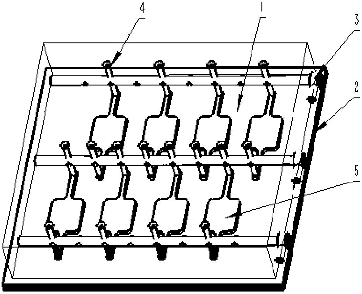
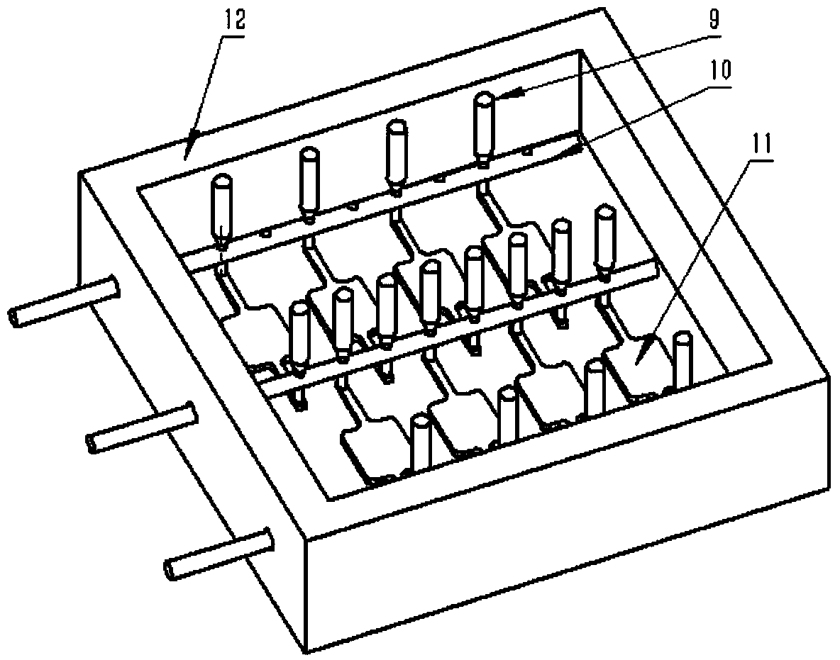
[0048] The cavity size of the combined mold is 33mm×32mm×7mm, the volume of the raised reaction chamber is 12uL, double-row structure, 4 in each row, a total of 8 reaction chambers, the channel is 0.4mm, the diameter of the mold cross column is 1mm, the mold The hole on the cross column is 0.3mm, the diameter of the mold column is 0.3mm, inject PDMS glue into the mold, heat and solidify, remove the mold column, take out the mold cross column, and fall off from the template to obtain a microchannel and reaction chamber. body substrate. The PDMS substrate and the 50mm×40mm glass substrate were cleaned by plasma to modify the surface and bonded to form a microfluidic chip. A 1.2mm rotating long rod with a handle is inserted into the die cross-column hole of the chip. The micro-holes on the mold cross-column are 0.3mm in size, and the micro-holes correspond to the channels generated by the mold post. At this time, the microfluidic chip is processed for biocompatibility, high temp...
example 2
[0050]The combined mold cavity size is 22mm×25mm×7mm, the volume of the raised reaction cavity is 20uL, single-row structure, 2 reaction chambers, the channel is 0.4mm, the diameter of the mold cross column is 1mm, and the hole on the mold cross column is 0.3mm, the diameter of the mold column is 0.3mm, inject PDMS glue into the mold, heat and cure, remove the mold column, take out the mold cross column, and fall off the template to obtain a substrate with microchannels and reaction chambers. The PDMS substrate and the 25mm×30mm glass substrate were cleaned by plasma to modify the surface and bonded to form a microfluidic chip. A 1.2mm rotating long rod with a handle is inserted into the die cross-column hole of the chip. The micro-holes on the mold cross-column are 0.3mm in size, and the micro-holes correspond to the channels generated by the mold post. At this time, the microfluidic chip is processed for biocompatibility, high temperature sterilization and other related proc...
PUM
 Abstract
Description
Claims
Application Information


