Transparent conductive ink, and method for producing transparent conductive pattern

A technology of transparent conductivity and material retention, applied in the direction of conductive pattern formation, transparent dielectrics, conductive materials dispersed in non-conductive inorganic materials, etc., can solve the problem of silver nanowire insulation difficulties, high manufacturing costs, waste of developer Eliminate problems such as liquids, and achieve the effect of suppressing manufacturing costs and environmental loads

Active Publication Date: 2015-01-21
OSAKA UNIV +1
View PDF15 Cites 13 Cited by
  • Summary
  • Abstract
  • Description
  • Claims
  • Application Information

AI Technical Summary

Problems solved by technology

[0032] In addition, the method of Patent Document 4 also requires a development process, so the silver nanowires are wasted due to development, and the problem of waste liquid of the developing solution also occurs.
[0033] Therefore, in order to obtain a transparent conductive film, many steps are required, and there are problems such as high manufacturing cost; problems of waste liquid generated from each step; and electrical and optical characteristics before and after each step are not optimized. Problems such as the accumulation of changes
[0034] In addition, the method of Patent Document 5 also has the following problems: it is very difficult to completely make the silver nanowires insulating during plasma treatment or corona treatment, and the base material is deteriorated by plasma treatment or corona treatment, and the transparency and durability deteriorate.
[0038] This method has the following problems: the design of both the hydrophobic transparent ink and the hydrophilic conductive ink is required, the blending system becomes complicated, and the pattern accuracy is greatly affected by the repellency between the hydrophobic and hydrophilic resins in addition to the printing accuracy. influence, so it is difficult to improve the pattern accuracy
In addition, it is difficult to uniformly press the film of conductive ink, and it is difficult to appear reproducible regarding the appearance of conductivity

Method used


Image

  • Transparent conductive ink, and method for producing transparent conductive pattern
  • Transparent conductive ink, and method for producing transparent conductive pattern
  • Transparent conductive ink, and method for producing transparent conductive pattern

Examples


Embodiment 1

[0112]

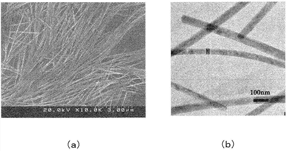
[0113] Polyvinylpyrrolidone K-90 (manufactured by Nippon Shokubai Co., Ltd.) (0.049 g), AgNO 3 (0.052g) and FeCl 3 (0.04 mg) was dissolved in ethylene glycol (12.5 ml), and the reaction was heated at 150°C for 1 hour. The obtained precipitate was isolated by centrifugation, and the precipitate was dried to obtain the target silver nanowire. exist figure 2 (a) and (b) show SEM images of the obtained silver nanowires. The SEM used was FE-SEM S-5200 manufactured by Hitachi High-Tech Corporation.

[0114] Depend on figure 2 (a) and (b), it can be seen that the silver nanowires are rod-shaped, and the diameter of the rod-shaped wires is about 70 nm, and the length is 10-20 μm, and the rod-shaped wires account for more than about 95% of the total. Furthermore, the remainder is granular.

[0115] The above ethylene glycol, AgNO 3 , FeCl 3 It is manufactured by Wako Pure Chemical Industry Co., Ltd.

[0116] In addition, the length and diameter of the silver nanow...

Embodiment 2、3

[0123] Except for changing the types and amounts of dibutyl ether, tersolub MTPH, and viscosity adjusting solvents in Example 1 to the amounts shown in Table 1, it was prepared in the same manner as in Example 1 so that the concentrations listed in Table 1 were obtained. transparent conductive ink.

Embodiment 4~7、9~13

[0125] As silver nanowires, instead of using the above-mentioned synthetic products, commercially available product SLV-NW-35 (isopropanol dispersion made by bluenano company, concentration is 10mg / ml, the diameter of silver nanowires is 35nm, and the length is about 15 μm ( catalog value)), a small amount of terpineol (manufactured by Nippon Terpen Chemical Co., Ltd.) was added to the silver nanowire dispersion to make it well dispersed, and then the isopropanol was distilled off and the solvent was replaced. Then, Tersolbu MTPH (manufactured by Nippon Terpen Chemical Co., Ltd., isobornylcyclohexanol) and terpineol were added so that the concentration of the final dispersion medium became the compounding ratio (mass ratio) described in Tables 1 to 3, and used ( Co., Ltd. ARV-310 manufactured by Shinky Co., Ltd. was well dispersed to obtain a dispersion liquid. In addition, the quantity of the small amount of terpineol which was added initially was calculated in advance and wa...


PUM

PropertyMeasurementUnit
viscosityaaaaaaaaaa
viscosityaaaaaaaaaa
viscosityaaaaaaaaaa

Abstract

[Problem] To provide: a transparent conductive ink which uses, as a conductive component, metal nanowire and/or metal nanotubes, and which can form a coating film that is both conductive and optically transparent; and a method for producing a transparent conductive pattern wherein the transparent conductive ink is used to create a transparent conductive pattern by means of easy manufacturing steps, the method having reduced manufacturing costs and environmental impact. [Solution] A transparent conductive ink in which metal nanowire and/or metal nanotubes are dispersed in a dispersion medium which comprises shape retaining material having a viscosity of 1.0 x 10³-2.0x10⁶ mPa.s at 25°C and comprising an organic compound having a molecular weight range of 150-500, and a method, for forming a transparent conductive pattern, using the transparent conductive ink to print an arbitrarily shaped pattern on a substrate, heat treating and drying same, and then irradiating pulsed light on the dried pattern.

Description

technical field [0001] The invention relates to a transparent conductive ink and a method for forming a transparent conductive pattern. Background technique [0002] Transparent conductive film, transparent electrode in liquid crystal display (LCD), plasma display panel (PDP), organic electroluminescence (OLED), solar cell (PV) and touch screen (TP), antistatic (ESD) film and electromagnetic wave shielding ( It is used in various fields such as EMI) thin films, and requires (1) low surface resistance, (2) high light transmittance, and (3) high reliability. [0003] For example, for a transparent electrode of an LCD, the surface resistance is in the range of 10 to 300Ω / □, and the light transmittance is 85% or more in the visible light region. In a more preferable range, the surface resistance is 20 to 100 Ω / □, and the light transmittance is 90% or more. For the transparent electrode of the OLED, the surface resistance is in the range of 10-100Ω / □, and the light transmittanc...

Claims


Application Information

Patent Timeline
Patent Type & Authority Applications(China)
IPC IPC(8): H01B1/22H05K1/09H05K3/00
CPCH01B1/22H05K1/097H05K3/1283H05K2203/107H05K2201/0108C09D11/52H05K2201/026C09D11/03H01B13/00H01B13/0016H01B13/003H05K3/12H01B13/0036
Inventor 菅沼克昭大冢邦显村桥浩一郎竹村康孝内田博
Owner OSAKA UNIV
Why Eureka
Try Eureka