A method for preparing nanochannels based on template-induced cracking effect
A technology of nano-flow channel and template, which is applied in the application of thermal effects to detect fluid flow, separation methods, chemical instruments and methods, etc., can solve the problems of long scanning time, technical difficulties, low processing efficiency, etc., and achieve good controllability and repeatability Sexuality, high efficiency and low cost
- Summary
- Abstract
- Description
- Claims
- Application Information
AI Technical Summary
Problems solved by technology
Method used
Image
Examples
example 1
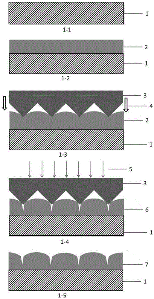
[0030] Such as figure 1 As shown in 1-1, select a piece of polydimethylsiloxane (PDMS) sheet 1 with a surface polishing thickness of 1 mm and an area of 2 cm × 2 cm, and use a mixture of alcohol and acetone to clean its surface , remove the stains on the surface, and dry it for later use;
[0031] Such as figure 1 As shown in middle 1-2, use the glue homogenizer, set the speed at 2000 rpm, spin-coat a layer of UV-curable mercapto-ene material 2 with a thickness of 150 nm on the PDMS plate, and the spin-coating accuracy is ±3 nm, The uniformity is ±3%;
[0032] Such as figure 1 As shown in 1-3, a piece of porous alumina with a pore diameter of 500 nm and an edge width of 30 nm is used as the imprint induction template 3, and the induction template 3 is gently attached to the sulfhydryl group by aligning the imprint process 4 -On the olefin material film layer 2, since PDMS is elastic, it can be in conformal contact with the template without external pressure, and no air b...
example 2
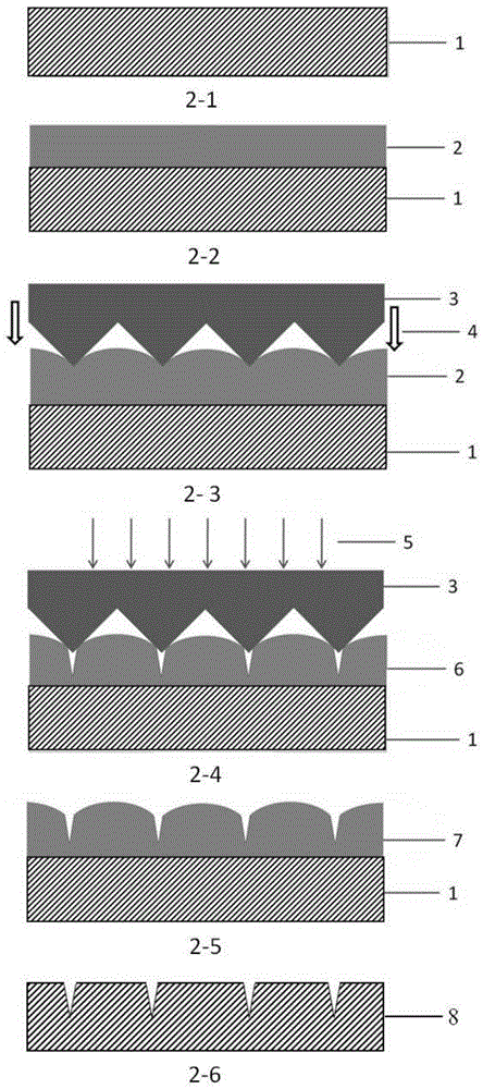
[0036] Such as figure 2 As shown in 2-1, select a single-sided polished silicon wafer with an area of 2 cm x 2 cm as the substrate 1, clean the surface with a mixture of alcohol and acetone, remove the stains on the surface, and dry it before use ;
[0037] Such as figure 2 As shown in middle 2-2, use the glue homogenizer, set the speed at 1500 rpm, spin-coat a layer of UV-curable mercapto-ene material 2 with a thickness of 200 nanometers on the PDMS plate, and the spin-coating accuracy is ±3 nanometers, The uniformity is ±3%;
[0038] Such as figure 2 As shown in 2-3, a ring-shaped microtip nanostructure with a period of 200 nanometers and a microtip size of 20 nanometers is used as the imprint induction template 3, and the induction template 3 is gently attached by aligning the imprint process 4 On the mercapto-ene material film layer 2, a pressure of 2 Pa is applied from the outside, so that the induced template 3 is in conformal contact with the material, and no a...
PUM
| Property | Measurement | Unit |
|---|---|---|
| thickness | aaaaa | aaaaa |
| width | aaaaa | aaaaa |
| depth | aaaaa | aaaaa |
Abstract
Description
Claims
Application Information


