A thick glue process for preparing tsv three-dimensional integrated rdl electroplating mask

A mask and process technology, applied in the field of microelectronics, can solve problems such as affecting the dimensional accuracy of electroplating patterns, increasing the thickness of secondary coating, and difficulty in obtaining an ideal adhesive film, so as to improve the reliability of electrical interconnection and improve surface uniformity. degree, the effect of improving the electrical interconnection characteristics

Active Publication Date: 2017-01-25
珠海天成先进半导体科技有限公司
View PDF6 Cites 0 Cited by
  • Summary
  • Abstract
  • Description
  • Claims
  • Application Information

AI Technical Summary

Problems solved by technology

But the main problem of this method is: AZ4620 has a limited coating thickness, which cannot meet the needs of electroplating RDL lines above 20 μm
But the main problems are: first, due to the fluidity of the photoresist, the morphology of the film is constantly changing, it is difficult to obtain an ideal film only by controlling the coating method, the process parameter window is not clear, and the film obtained by this method The internal stress of the layer is relatively large; the second is that the second glue coating is directly carried out without baking after the first glue coating. If the speed is not controlled properly, a large part of the surface glue will be thrown out, which will eventually lead to an insignificant increase in the thickness of the second glue coating, which is difficult to Fabrication of Thick Adhesive Masks Required for RDL Plating of TSV Stereo Integration
However, the disadvantages of making RDL electroplating mask by this method are as follows: First, there is a large internal stress in SU-8 thick glue, especially for ultra-thin wafers with a thickness less than 100 μm in TSV three-dimensional integration, when its thickness is close to the thickness of the glue layer Severe bending or even slivers will occur; the second is that the thermal expansion effect of SU-8 glue in the electroplating solution will cause the line width of the electroformed structure to decrease, which seriously affects the accuracy of the electroplating pattern size; the third is that after the baking process, the SU-8 -8 glue will be highly cross-linked and difficult to be completely removed
However, the problems of this method are as follows: firstly, it is difficult to ensure high-quality outline structure lines by two times of photolithography and electroplating, and the process is relatively cumbersome; The height of the mask after engraving is inconsistent, and it is difficult to ensure the flatness of the surface after overflow plating; third, this method has strict requirements on the height difference between the surface of the electroplating structure and the photoresist, and requires a high degree of process control, resulting in Low preparation efficiency
[0006] Therefore, the existing thick mask preparation technology cannot meet the requirements of RDL electroplating in TSV three-dimensional integration for thicker, higher uniformity, and steep sidewall masks, and the removal of glue is cumbersome, and it cannot be compatible with the TSV three-dimensional integration process. The disadvantage of high cost,

Method used


Image

  • A thick glue process for preparing tsv three-dimensional integrated rdl electroplating mask
  • A thick glue process for preparing tsv three-dimensional integrated rdl electroplating mask
  • A thick glue process for preparing tsv three-dimensional integrated rdl electroplating mask

Examples


example 1

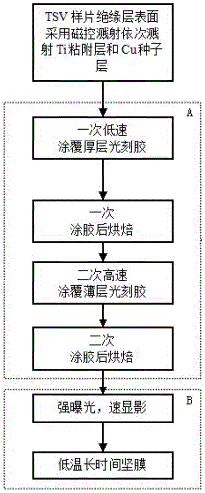
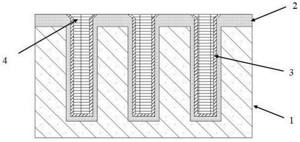
[0038]This embodiment is used to make a high RDL line electroplating mask on the surface of the insulating layer of the TSV blind via electroplating wafer, the average thickness of the mask is 25.96 μm, and the TTV is less than 1.5 μm. Such as figure 2 As shown, the TSV blind hole electroplating operation wafer adopts Si substrate 1, and SiO is arranged between the blind hole and Si substrate 1. 2 Insulating layer 2, the wall of the blind hole is provided with Ti adhesion layer 3 and Cu column 4 sequentially from outside to inside, and the implementation steps of its electroplating mask are as follows, as figure 1 Shown:

[0039] Step 1. First, use acetone and isopropanol to ultrasonically clean the operating wafer for 5 minutes respectively to remove the polishing liquid particles and impurities remaining in the CMP process; 2 On the insulating layer 2, a 100nm Ti adhesion layer 3 and a 600nm Cu seed layer, namely the UBM layer, are sequentially sputtered, such as image ...

example 2

[0052] The present invention is a thick glue process for preparing TSV three-dimensionally integrated RDL electroplating mask, and the specific process steps are as follows:

[0053] Step 1, one glue coating is divided into two steps: Step1 rotates at 600rpm, spin coating time is 5s, and acceleration is 6000rpm / s; Step2 rotates at 1000rpm, spins for 30s, and accelerates at 10000rpm / s.

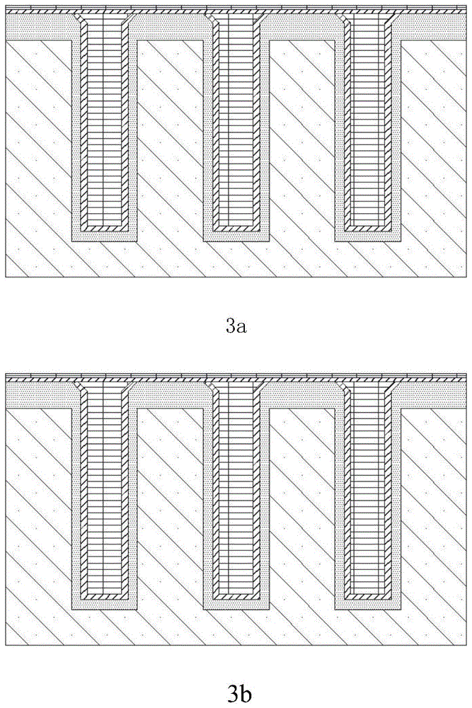
[0054] Step 2: Baking after coating once, the baking temperature is 100°C, and the baking time is 3 minutes, such as image 3 As shown in b, the time interval between primary baking and secondary gluing is 1min.

[0055] Step 3, the second glue coating is divided into three steps: Step1 is 400rpm, time is 4s, acceleration is 6000rpm / s; Step2 is 1000rpm, time is 4s, acceleration is 8000rpm / s; Step3 is 3000rpm, spin coating The time is 40s and the acceleration is 10000rpm / s.

[0056] Step 4, bake after the second glue coating, the baking temperature is 100°C, and the baking time is 7 minutes, s...

example 3

[0060] The present invention is a thick glue process for preparing TSV three-dimensionally integrated RDL electroplating mask, and the specific process steps are as follows:

[0061] Step 1, one glue application is divided into two steps: Step1 rotates at 500rpm, spin coating time is 6s, and acceleration is 6000rpm / s; Step2 rotates at 1000rpm, spins for 35s, and accelerates at 10000rpm / s.

[0062] Step 2: Baking after coating once, the baking temperature is 100°C, and the baking time is 3 minutes, such as image 3 As shown in b, the time interval between primary baking and secondary gluing is 1min.

[0063] Step 3, the second glue coating is divided into three steps: Step1 rotates at 400rpm, time is 3s, acceleration is 6000rpm / s; Step2 rotates at 1300rpm, time is 5s, acceleration is 8000rpm / s; Step3 rotates at 4000rpm, spin coating The time is 35s and the acceleration is 10000rpm / s.

[0064] Step 4, bake after the second glue coating, the baking temperature is 100°C, and the...


PUM

PropertyMeasurementUnit
thicknessaaaaaaaaaa
thicknessaaaaaaaaaa
thicknessaaaaaaaaaa

Abstract

The invention discloses a thick-film coating process for preparing a TSV three-dimensional integrated RDL electroplated mask. The technology comprises the following steps: a Ti adhesion layer and a Cu seed layer are sequentially sputtered on the surface of an insulated layer of a TSV blind hole electroplated wafer; a thick film is prepared in a mode of gluing for two times and baking for two times, a thick photoresist is coated at low speed for the first time, a thin photoresist is coated at high speed for the second time, time and temperature of the two-time baking vary according to the thickness ratio of the upper glue layer to the lower glue layer, and the ratio of the accumulated baking time of the bottom glue layer to the baking time of the surface glue layer is the thickness ratio of the two; and exposure, development and hardbaking are then carried out for preparing the RDL electroplated mask. Through adjusting parameters of two-time gluing and conditions of baking, uniformity of the thick film layer and resolution of lithography can be ensured; through strong exposure, quick development and low-temperature and long-time hardbaking, the mask which is high in precision, steep in side wall, higher in thickness and higher in uniformity can be manufactured; and the technology of the invention can be applied to RDL interconnecting wire whose electroplated layer is higher than 20mum and appearance is clear and neat.

Description

technical field [0001] The invention belongs to the technical field of microelectronics, in particular to a thick glue process for preparing a TSV three-dimensionally integrated RDL electroplating mask. Background technique [0002] At present, the RDL wiring used in TSV three-dimensional integration is generally prepared by electroplating process. The quality of the mask in the electroplating process is the key to realizing high-quality RDL. In order to improve the electrical interconnection characteristics of ultra-thin wafers and TC( The reliability of Thermal cycling) and HTS (High Temperature Storage) requires the thickness of RDL lines to be as high as 20 μm or more. However, to prepare such a thick electroplating mask, the uniformity of the mask, the photolithographic resolution, and the steepness of the sidewall will be the key factors affecting the RDL electroplating process. [0003] "Research on AZ4620 Thick Resist Photolithography Process for Micro Device Proces...

Claims


Application Information

Patent Timeline
Patent Type & Authority Patents(China)
IPC IPC(8): H01L21/02H01L21/60G03F7/20
Inventor 张巍单光宝袁海刘松
Owner 珠海天成先进半导体科技有限公司
Why Eureka
Try Eureka