Unlock instant, AI-driven research and patent intelligence for your innovation.

Complementary tunneling field effect transistor and manufacturing method thereof

A technology of tunneling field effect and manufacturing method, which is applied in the field of complementary tunneling field effect transistor and its manufacturing, and can solve the problems of uneven ion distribution and low carrier tunneling efficiency

Active Publication Date: 2015-02-04
HUAWEI TECH CO LTD
View PDF5 Cites 11 Cited by
  • Summary
  • Abstract
  • Description
  • Claims
  • Application Information

AI Technical Summary

Problems solved by technology

[0004] Since the existing technology uses ion implantation to dope the source region and drain region of the tunneling field effect transistor with impurities, but the impurity concentration distribution formed by the ion implantation process in the source region and the drain region is generally a Gaussian distribution, so the ion implantation process is used When the ions are distributed unevenly, it is difficult to form a tunnel junction with sudden doping, so under the action of a certain gate electric field, the tunneling efficiency of carriers is relatively low.

Method used


Image

  • Complementary tunneling field effect transistor and manufacturing method thereof
  • Complementary tunneling field effect transistor and manufacturing method thereof
  • Complementary tunneling field effect transistor and manufacturing method thereof

Examples


Embodiment 1

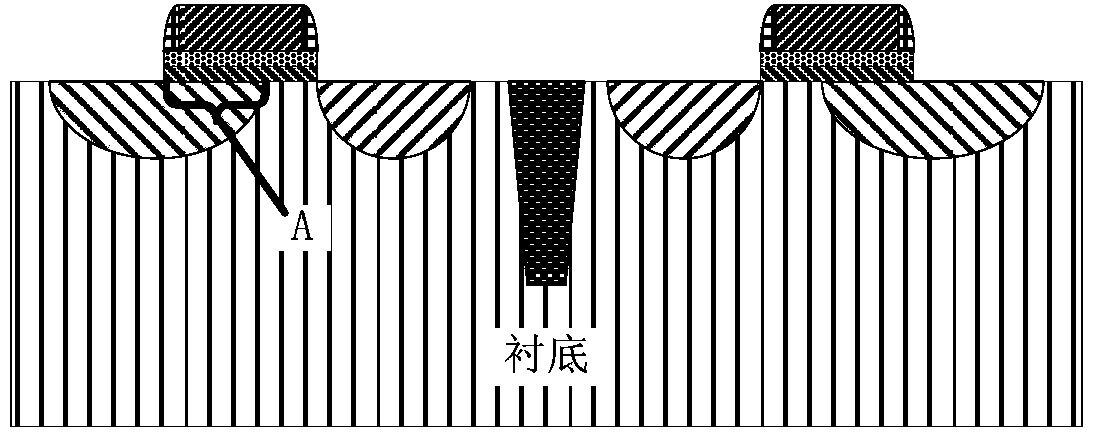
[0048] An embodiment of the present invention provides a complementary tunneling field effect transistor, such as figure 2 Shown is a schematic structural diagram of the tunneling field effect transistor.

[0049] The tunneling field effect transistor includes: a substrate 10; a first drain region 20a and a first source region 20b disposed on the substrate 10, the first drain region 20a and the first source region 20b include a first dopant; The first channel 30a on the first drain region 20a and the second channel 30b disposed on the first source region 20b; the second source region 40a disposed on the first channel 30a and the second channel disposed on the second channel The second drain region 40b on 30b, the second source region 40a and the second drain region 40b include the second dopant; the first epitaxial layer 50a disposed on the first drain region 20a and the second source region 40a, and the The second epitaxial layer 50b on the second drain region 40b and the f...

Embodiment 2

[0073] An embodiment of the present invention provides a method for manufacturing a complementary tunneling field effect transistor, such as Figure 7 Shown is a schematic flow chart of the preparation method.

[0074] S101. Deposit a first doped layer on a substrate.

[0075] Such as Figure 8 Substrate 10 is shown. What needs to be added is that the substrate 10 may be a semiconductor substrate, and the specific material of the substrate 10 may be germanium, silicon, silicon germanium or a group III-V compound.

[0076] Such as Figure 9 As shown, a first doped layer 20 is deposited on a substrate 10 .

[0077] It should be noted that the first doped layer 20 includes a first dopant, the first dopant is doped in the semiconductor thin film, and the concentration of the first dopant is higher than 10 per cubic centimeter. 19 pcs, between 10 per cubic centimeter 19 to 10 per cubic centimeter 21 between. Wherein, the material of the semiconductor thin film is germanium,...


PUM


Abstract

The embodiment of the invention provides a complementary tunneling field effect transistor and a manufacturing method thereof, and relates to the technical field of semiconductors. The complementary tunneling field effect transistor is able to improve the tunneling efficiency of charge carrier, so as to improve the performance of the complementary tunneling field effect transistor. The transistor comprises a first drain area, a first source area, a first channel, a second channel, a second source area, a second drain area, first extension layers, second extension layers, a first gate stacking layer and a second gate stacking layer, wherein the first drain area and the first source area both comprise first inclusions; the first channel is arranged on the first drain area; the second channel is arranged on the first source area; the second source area is arranged on the first channel; the second drain area is arranged on the second channel; the second source area and the second drain area both comprise second inclusions; the first extension layers are arranged on the first drain area and the second source area; the second extension layers are arranged on the second drain area and the first source area; the first gate stacking layer is arranged on the first extension layer; the second gate stacking layer is arranged on the second extension layer.

Description

technical field [0001] The invention relates to the technical field of semiconductors, in particular to a complementary tunneling field effect transistor and a manufacturing method thereof. Background technique [0002] With the evolution of the transistor manufacturing process, the size of the transistor continues to shrink. However, in the process of shrinking the size of the transistor to close to the physical limit, the transistor also faces many problems, such as serious short-channel effect, large leakage current, and high power density. . Aiming at these problems, various solutions have been proposed in the industry. Among them, TFET (Tunnel Field Effect Transistor, Tunneling Field Effect Transistor) is not affected by MOSFET (Metal Oxide Semiconductor Field Effect Transistor, Metal Oxide Semiconductor Field Effect Transistor) sub- Advantages such as limitation of threshold swing have received widespread attention. [0003] Existing Tunneling Field Effect Transisto...

Claims


Application Information

Patent Timeline
Patent Type & Authority Applications(China)
IPC IPC(8): H01L29/78H01L29/08H01L21/336
CPCH01L21/823814H01L27/092H01L29/0847H01L29/7391H01L29/42356H01L29/66356H01L29/0676H01L21/823828H01L21/823878H01L21/823885H01L29/78642H01L29/78681H01L29/78696H01L29/78H01L29/08H01L21/823807H01L29/0653H01L29/42392H01L29/4908H01L29/66977H01L29/78618H01L29/78651H01L29/78684
Inventor 杨喜超赵静张臣雄
Owner HUAWEI TECH CO LTD