Patterned substrate preparation method and epitaxial wafer production method
A patterned substrate and patterned technology, which is applied in semiconductor/solid-state device manufacturing, electrical components, circuits, etc., can solve the problems of low light reflectivity, improve light reflectivity, reduce defects and dislocations, and improve light output. efficiency effect
- Summary
- Abstract
- Description
- Claims
- Application Information
AI Technical Summary
Problems solved by technology
Method used
Image

Examples
Embodiment 1
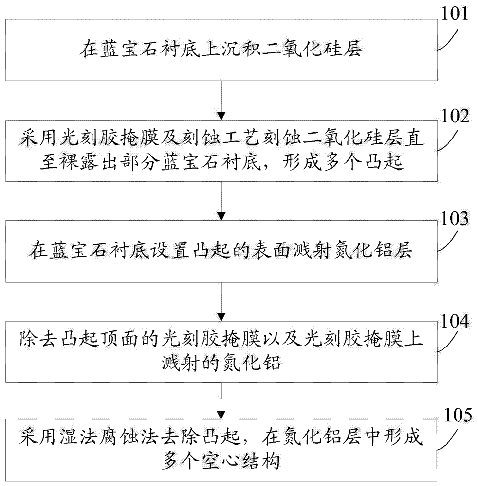
[0042] The embodiment of the present invention provides a method for preparing a patterned substrate, see figure 1 , The method includes:
[0043] Step 101: Deposit a silicon dioxide layer on a sapphire substrate.
[0044] In this embodiment, depositing a silicon dioxide layer on a sapphire substrate includes:
[0045] A plasma-enhanced chemical vapor deposition method or a sol-gel method is used to deposit a silicon dioxide layer on the sapphire substrate.
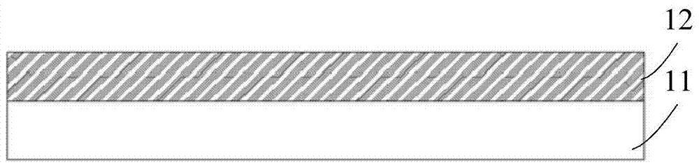
[0046] Such as figure 2 As shown, a silicon dioxide layer 12 is deposited on the sapphire substrate 11.
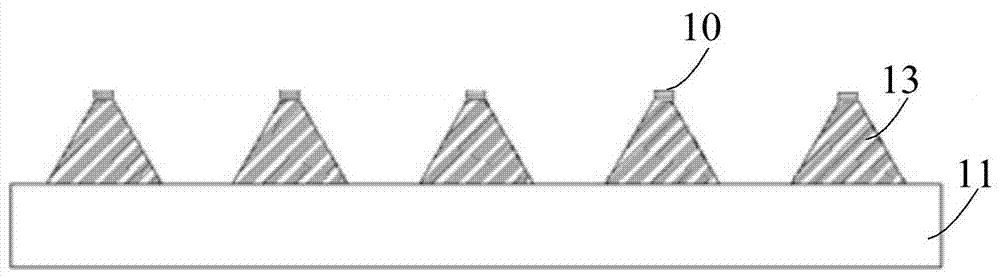
[0047] Step 102: Use a photoresist mask and an etching process to etch the silicon dioxide layer until a part of the sapphire substrate is exposed to form a plurality of protrusions. The protrusions have a mesa structure and a photoresist mask is left on the top surface of the protrusions membrane.
[0048] Specifically, the protrusion may be one or more of a truncated cone structure, an elliptical cone structure, and a prism ...
Embodiment 2
[0066] The embodiment of the present invention provides a method for manufacturing an epitaxial wafer, see Figure 7 , The method includes:
[0067] Step 201: Prepare a patterned substrate according to the method in the first embodiment.
[0068] Step 202: sequentially growing an n-type gallium nitride layer, a multiple quantum well layer and a p-type gallium nitride layer on the patterned substrate to form an epitaxial wafer.
[0069] Specifically, the side epitaxial growth method is used to sequentially grow an n-type gallium nitride layer, a multiple quantum well layer, and a p-type gallium nitride layer on a patterned substrate to form an epitaxial wafer.
[0070] In the embodiment of the present invention, a silicon dioxide layer is deposited on a sapphire substrate, a plurality of protrusions are etched using a photoresist mask and an etching process, and an aluminum nitride layer is sputtered on the surface of the sapphire substrate. The protrusions are removed by wet etching t...
Embodiment 3
[0072] The embodiment of the present invention provides a patterned substrate, see Figure 8 , The substrate includes:
[0073] A sapphire substrate 301 and an aluminum nitride layer 302 disposed on the sapphire substrate 301. A plurality of hollow structures 302a are provided in the aluminum nitride layer 302, and the hollow structures 302a are mesa structures.
[0074] Specifically, the hollow structure 302a may be one or more of a truncated cone structure, an elliptical cone structure, and a prism cone structure.
[0075] Further, the radius or width of the top surface of the hollow structure 302a is 0.05-0.5um, the radius or width of the bottom surface of the hollow structure 302a is 0.5-10um, and the height of the hollow structure 302a is 0.5-5um. The hollow structure of this size has an obvious effect on reflectivity and can maximize the efficiency of LED light.
[0076] In this embodiment, a plurality of hollow structures 302a are arranged in a matrix to form a periodic pattern...
PUM
| Property | Measurement | Unit |
|---|---|---|
| refractive index | aaaaa | aaaaa |
| refractive index | aaaaa | aaaaa |
| refractive index | aaaaa | aaaaa |
Abstract
Description
Claims
Application Information