Phase change memory gate tube and storage unit of phase change memory gate tube

A phase-change memory and strobe technology, which is applied in electrical components, semiconductor devices, electric solid-state devices, etc., can solve the problems of increasing storage unit area, reducing storage density and integration, and increasing power consumption.

Inactive Publication Date: 2015-02-11
QUFU NORMAL UNIV
View PDF5 Cites 8 Cited by
  • Summary
  • Abstract
  • Description
  • Claims
  • Application Information

AI Technical Summary

Problems solved by technology

In order to obtain a large enough drive current to ensure the normal operation of all memory cells, the gating tube of each memory cell must also be...

Method used


Image

  • Phase change memory gate tube and storage unit of phase change memory gate tube
  • Phase change memory gate tube and storage unit of phase change memory gate tube
  • Phase change memory gate tube and storage unit of phase change memory gate tube

Examples


Embodiment 1

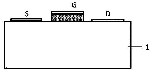
[0037] 1. Using photolithography method on MoS 2 MoS-based 2 MOSFETs;

[0038] 2. In MoS 2 Preparation of 50~300nm thick SiO on MOSFET 2 medium layer;

[0039] 3. Using photolithography method on MoS 2 SiO with a diameter of 100nm~1000nm is prepared at the drain end (D end) of the MOSFET 2 media layer graphics;

[0040] 4. Using electron beam lithography and etching technology on the above D-terminal SiO 2 A hole with a diameter of 50nm~500nm is prepared in the dielectric layer, and the bottom end of the hole is connected to the MoS 2 The D terminal of the MOSFET is connected;

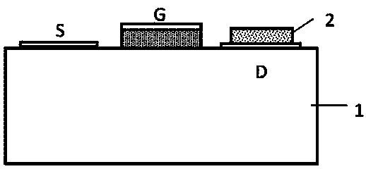
[0041] 5. Use ALD technology to fill W in the above hole, after the hole is filled, use CMP to remove the W material outside the hole mouth to form a columnar W pattern;

[0042] 6. Use magnetron sputtering to deposit the phase change material GeSbTe and the buffer layer TiN, the thickness of the phase change material is 50~200 nm, and the thickness of TiN is 10~50 nm;

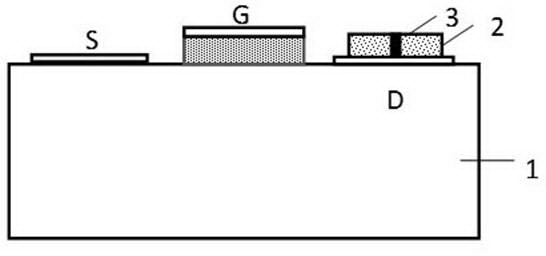
[0043] 7. Using Ph...

Embodiment 2

[0046] 1. Using photolithography method on MoS 2 MoS-based 2 MOSFETs;

[0047] 2. In MoS 2 Preparation of 50~300nm thick SiO on MOSFET 2 medium layer;

[0048] 3. Using photolithography method on MoS 2 SiO with a diameter of 100nm~1000nm is prepared at the drain end (D end) of the MOSFET 2 media layer graphics;

[0049] 4. Using electron beam lithography and etching technology on the above D-terminal SiO 2 A hole with a diameter of 50nm~500nm is prepared in the dielectric layer, and the bottom end of the hole is connected to the MoS 2 The D terminal of the MOSFET is connected;

[0050] 5. Use ALD technology to fill TiN in the above hole. After the hole is filled, use CMP to throw away the TiN material other than the hole mouth to form columnar TiN. Using TiN as the heating electrode can achieve better heating effect and improve the heating electrode. Interface properties with phase change materials;

[0051] 6. Use magnetron sputtering to deposit the phase change ...

Embodiment 3

[0055] 1. Using photolithography method on MoS 2 MoS-based 2 MOSFETs;

[0056] 2. In MoS 2 Preparation of 50~300nm thick SiO on MOSFET 2 medium layer;

[0057] 3. Using photolithography method on MoS 2 SiO with a diameter of 100nm-1000nm is prepared at the drain end (D end) of the MOSFET 2 media layer graphics;

[0058] 4. Using electron beam lithography and etching technology on the above D-terminal SiO 2 A hole with a diameter of 50nm~500nm is prepared in the dielectric layer, and the bottom end of the hole is connected to the MoS 2 The D terminal of the MOSFET is connected;

[0059] 5. Use ALD technology to fill W in the above holes. After the holes are filled, use CMP to remove the W material outside the hole mouth to form a columnar W pattern;

[0060] 6. Use magnetron sputtering to deposit phase change material TiSbTe and buffer layer TiN. The thickness of the phase change material is 50-200 nm, and the thickness of TiN is 10-50 nm; using TiSbTe material can ...


PUM

PropertyMeasurementUnit
Diameteraaaaaaaaaa
Thicknessaaaaaaaaaa

Abstract

A phase change storage technology is a new generation of storage technology with excellent performance, the technical node limitation is avoided, when the size is smaller, the performance is more excellent, the speed is higher, and the power consumption is lower. The invention provides a phase change memory device unit, which consists of a field effect tube and a variable-resistant element based on a chalcogenide compound material, wherein an MoS2 field effect tube is used as a gate tube, and the chalcogenide compound variable-resistant element realizes the information storage. The MoS2 is a ultra-thin two-dimensional chalcogenide compound semiconductor material, the MoS2 field effect tube has smaller size and lower energy consumption than the conventional silicon field effect tube, the power consumption is only hundred thousandth of that of the silicon material according to reports in the prior art, the room temperature migration rate reaches 200 cm<2>/Vs, and the room temperature current switch ratio reaches 108. The MoS2 field effect tube and the chalcogenide compound variable-resistant element are combined for forming a phase change memory device unit, and the low-power-consumption high-speed and high-density phase change memory can be realized.

Description

technical field [0001] The invention relates to a novel device unit for high-speed, low-power consumption, and high-density phase-change storage. In view of the current status and the technical bottlenecks faced by Si semiconductor technology, a MoS 2 The field effect transistor is used as the phase change memory device unit of the gate transistor. The phase-change memory device unit consists of a nano-MoS-based 2 Material field effect transistors and resistive switching elements based on chalcogenide materials, in which MoS 2 The field effect transistor is used as a gate tube, and the chalcogenide resistive element realizes information storage. MoS 2 The phase-change memory device unit formed by combining field effect transistors and chalcogenide resistive elements can realize low-power consumption, high-speed, and high-density phase-change memory. The invention belongs to the field of novel devices and techniques in microelectronics. Background technique [0002] Amo...

Claims


Application Information

Patent Timeline
IPC IPC(8): H01L45/00H01L27/24
Inventor 韩培高钱波吴良才宋志棠孟云
Owner QUFU NORMAL UNIV
Why Eureka
Try Eureka