Silicon dioxide plated nanometer particle pinhole filling method

A nanoparticle, silicon dioxide technology, applied in Raman scattering, material excitation analysis, etc., can solve the problems of unsuitable SHINERS detection, reduced SHINERS activity, easy existence of pinholes in the shell, etc., to achieve mass storage and application. , The effect of effectively removing pinholes and low shell thickness

Inactive Publication Date: 2015-03-04
XIAMEN UNIV
View PDF5 Cites 6 Cited by
  • Summary
  • Abstract
  • Description
  • Claims
  • Application Information

AI Technical Summary

Problems solved by technology

When SiO 2 When the shell thickness is less than 4nm, the SHINERS activity is relatively high, but the shell is prone to pinholes, which is not suitable for SHINERS detection; when the shell thickness is greater than 4nm, although the shell has no pinholes, the SHINERS activity is already greatly reduce

Method used


Image

  • Silicon dioxide plated nanometer particle pinhole filling method
  • Silicon dioxide plated nanometer particle pinhole filling method
  • Silicon dioxide plated nanometer particle pinhole filling method

Examples


Embodiment 1

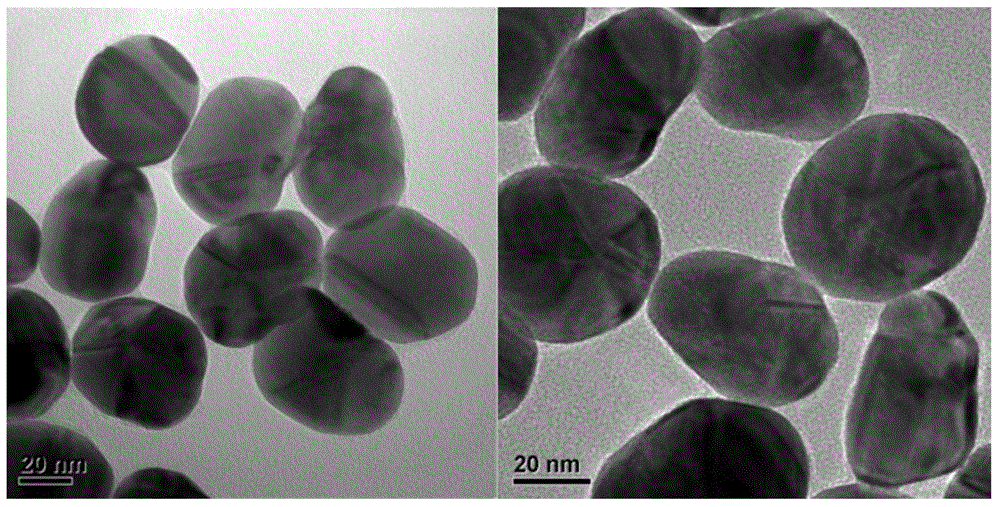
[0027] Take gold nanoparticles with a size of 55nm and a core-shell structure nanoparticle with a silica shell of 2nm as an example to fill pinholes.

[0028] Heat 100ml of chloroauric acid aqueous solution with a mass fraction of 0.01% to boiling, and quickly add 0.7ml of an aqueous solution of sodium citrate with a mass fraction of 1%. After about 2 to 3 minutes, the solution gradually turns from light yellow to black and then red Brown, continue to slightly boil for 40 minutes, stop the reaction, and cool to room temperature to obtain 55nm gold nanoparticles. Get 30ml 55nm gold nanoparticle sol, add 0.4ml 1mM 3-aminopropyltrimethoxysilane (APTMS) aqueous solution, stir for 15min, then add 3ml 0.54% sodium silicate solution, use 0.1M HCl solution to adjust the pH to 9.5, continue stirring for 3 minutes. Then place the reaction vessel in a water bath at 95°C and heat it for 20 minutes to obtain 55nm Au2nm SiO with pinholes 2 Nanoparticles. Take 10ml 55nm Au2nm SiO 2 The n...

Embodiment 2

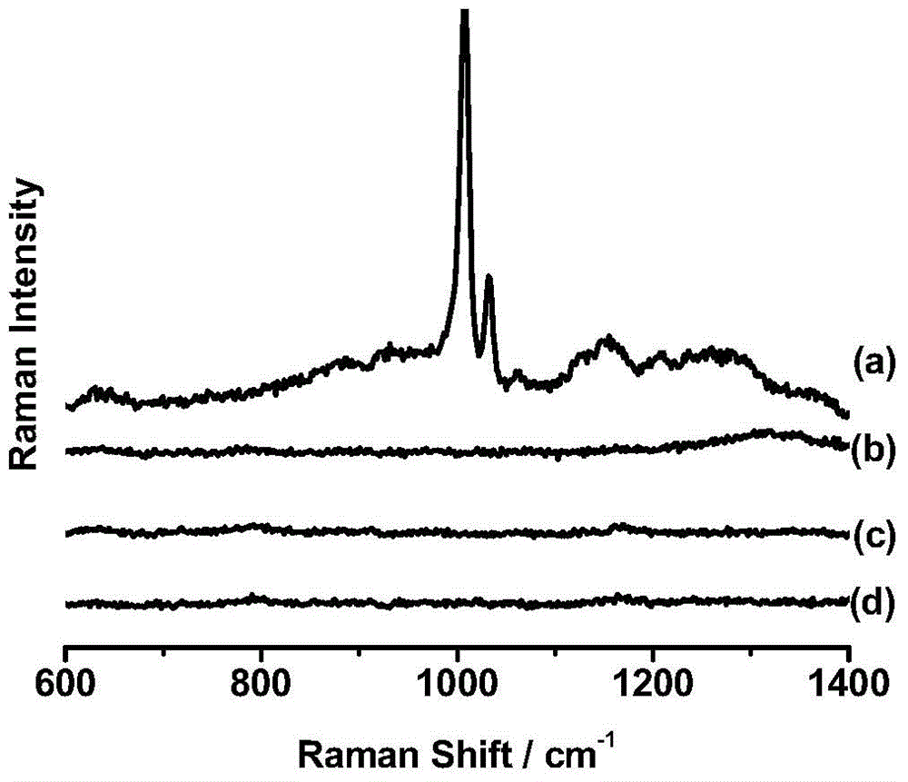
[0030] Example 2 Nanoparticle pinhole detection

[0031] With different AuSiO 2 An example of Raman detection of 10mM pyridine on a nanoparticle-modified silicon wafer as a substrate.

[0032] The centrifuged AuSiO 2Nanoparticles were added dropwise on a silicon wafer cleaned with a 3:1 mixed solution of concentrated sulfuric acid and hydrogen peroxide, and dried in vacuum to obtain a substrate sample. Add a drop of 10mM pyridine solution dropwise on the prepared sample, and test with a large-scale Raman tester to obtain the Raman signal of pyridine on the nanoparticle (see figure 2 ).

[0033] From figure 2 (a) It can be seen that in 55nm Au2nm SiO 2 A strong pyridine signal appeared on the nanoparticles, indicating that the nanoparticles were indeed pinholes. By joining S 2- After filling the pinhole, the pyridine signal disappeared immediately ( figure 2 b–d), showing that the pinholes have been filled with high efficiency.

Embodiment 3

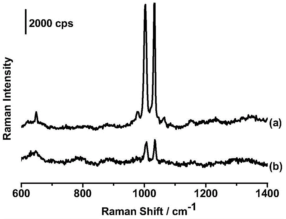
[0034] Example 3 SHINERS Enhanced Detection

[0035] Take the SHINERS detection of pyridine on a smooth Ag electrode as an example.

[0036] The different SHINERS nanoparticles after centrifugation were added dropwise on the smooth silver electrode and dried in vacuum; then the smooth silver electrode was placed in a Raman electrolytic cell containing 10mM pyridine, the selected laser power was 3mW, and the laser wavelength was 633nm. Get the SHINERS signal spectrum of pyridine on the smooth Ag electrode (see image 3 ).

[0037] It can be seen from the figure that 55nm Au2nm SiO filled with pinholes 2 Nanoparticles with pinhole-free 55nm Au4nm SiO 2 The SHINERS activity of nanoparticles is different. The signal intensity of the former is about 6-7 times higher than that of the latter, and the thickness of the shell is consistent with the reflected signal intensity, which fully proves that the use of S 2- Feasibility of filling the pinhole method.


PUM

PropertyMeasurementUnit
thicknessaaaaaaaaaa
thicknessaaaaaaaaaa

Abstract

The invention discloses a silicon dioxide plated nanometer particle pinhole filling method and relates to a shell optimization method for core-shell structure nanometer particles. The silicon dioxide plated nanometer particle pinhole filling method includes that 1) synthesizing or selecting Au@SiO2 nanometer particles with pinholes in the shells; 2) adding sulfide capable of dissociating S2- in water to Au@SiO2 nanometer particle sol to vulcanize the surfaces of the Au@SiO2 nanometer particles to enable the pinholes to disappear. The silicon dioxide plated nanometer particle pinhole filling method is simple, quick and effective. The core-shell structure nanometer particles without pinholes can be obtained through carrying out sulfide treatment on the silicon dioxide plated nanometer particles with pinholes. The silicon dioxide plated nanometer particle pinhole filling method is important for the nanometer particle synthesis, shell isolation nanometer particle reinforcing Raman spectrum (SHINERS) and the like.

Description

technical field [0001] The invention relates to a shell layer optimization technology of nanoparticles with a core-shell structure, in particular to a technology for filling shell pinholes with sulfide. Background technique [0002] Surface-enhanced Raman scattering (SERS) is a powerful spectroscopic technique, which has good surface selectivity and single-molecule level detection sensitivity, and is widely used in solid surface, biological analysis and chemical analysis. However, only three metals, Au, Ag, and Cu, have high SERS activity, and only rough and nanostructured surfaces are active SERS substrates, which severely limits the application range of SERS technology. In the past 40 years, various technologies and methods have been developed, such as electrochemical roughening, regular nanoarrays, transition metal core-shell nanoparticles, tip-enhanced Raman spectroscopy (TERS), etc., to a certain extent expand the universality of SERS substrates. sex. In 2010, J.F.Li ...

Claims


Application Information

Patent Timeline
Patent Type & Authority Applications(China)
IPC IPC(8): B22F1/00G01N21/65
Inventor 林晓东刘娜田中群
Owner XIAMEN UNIV
Why Eureka
Try Eureka