Oxygen-doped amorphous silicon germanium film, heterojunction crystalline silicon solar cell and manufacturing method
A technology of amorphous silicon germanium and crystalline silicon, which is applied in the field of solar cells and manufacturing, can solve the problems of increasing band gap discontinuity and affecting the collection of hole carriers, and achieve narrow band gap, effective collection, and suppression of epitaxy Effect
- Summary
- Abstract
- Description
- Claims
- Application Information
AI Technical Summary
Problems solved by technology
Method used
Image
Examples
Embodiment 1
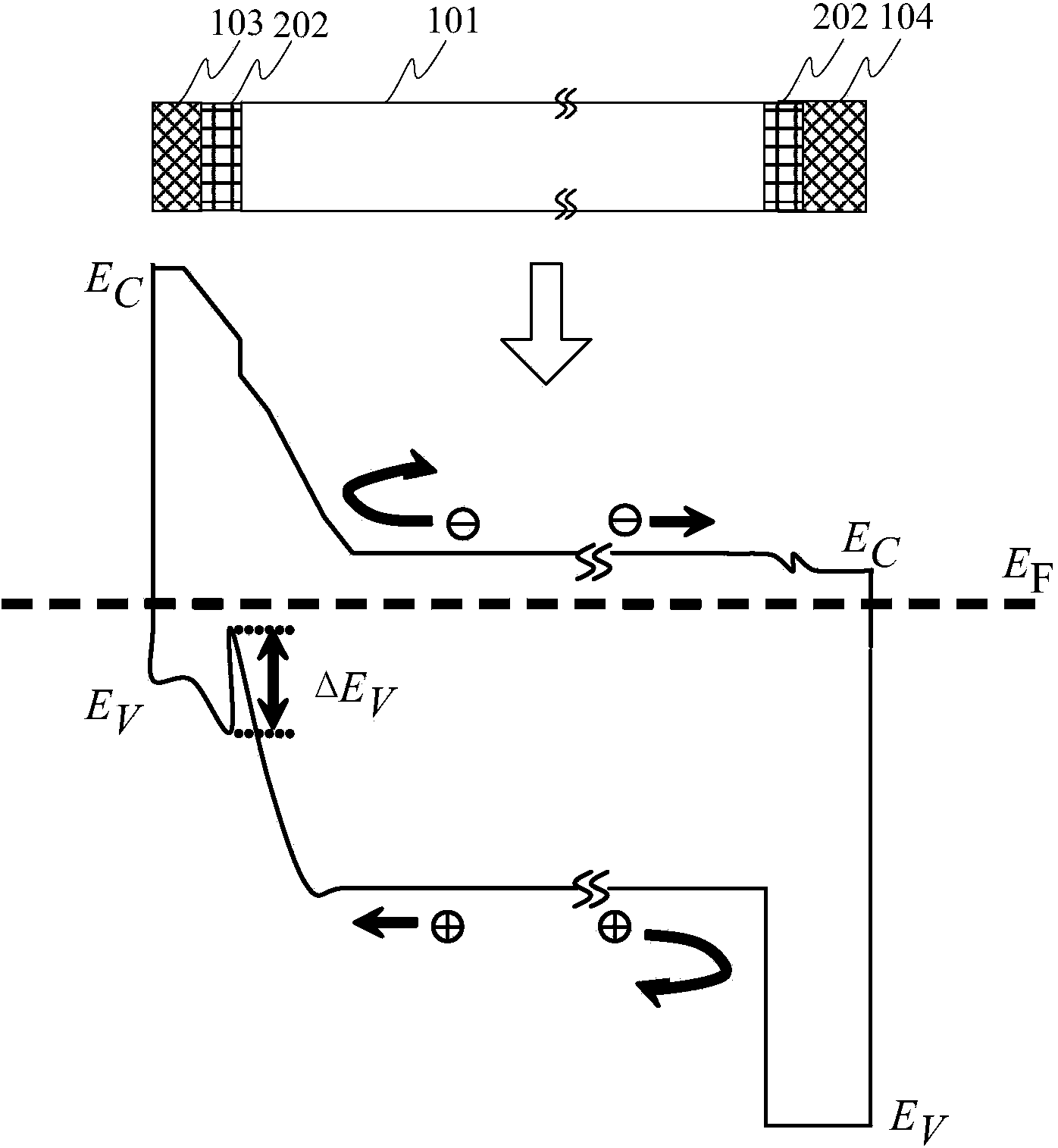
[0039] Such as figure 2As shown, the present embodiment provides a method for preparing an oxygen-doped amorphous silicon germanium film 202 for passivating the surface of crystalline silicon. The preparation method includes the steps of: providing a crystalline silicon substrate 101, on which An oxygen-doped amorphous silicon germanium film 202 is deposited on the surface of the bottom 101 .
[0040] As an example, an oxygen-doped amorphous silicon germanium film 202 is deposited on the surface of the crystalline silicon substrate 101 by using a chemical vapor deposition process. Wherein, the chemical vapor deposition process includes a plasma chemical vapor deposition process and a hot wire chemical vapor deposition process.
[0041] As an example, the reaction gases used in the chemical vapor deposition process include germanium source gas, silicon source gas, oxygen source gas and diluent gas. Further, the germanium source gas includes GeH 4 、GeF 4 and GeH 3 CH 3 On...
Embodiment 2
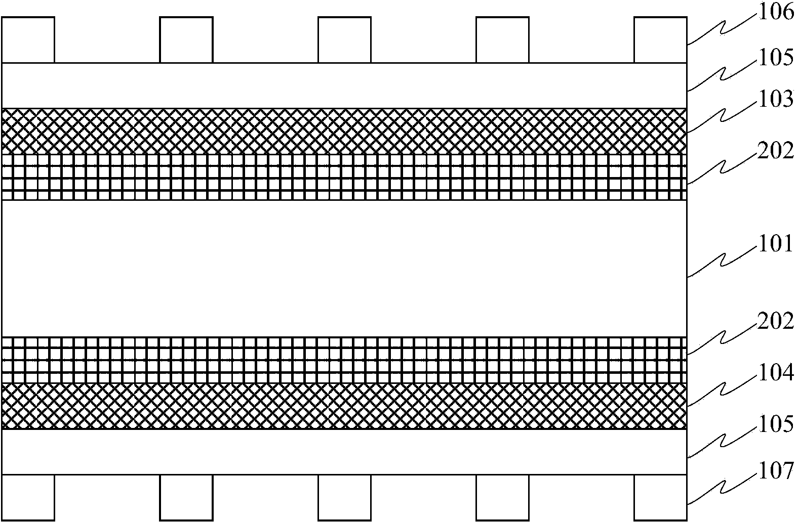
[0051] Such as image 3 As shown, this embodiment provides a method for preparing a heterogeneous crystalline silicon solar cell, including steps:
[0052] 1) Provide an N-type crystalline silicon substrate 101, place the crystalline silicon substrate 101 in a reaction chamber, and make the reaction chamber have a preset background vacuum degree. In this embodiment, a smooth or velvety crystalline silicon substrate 101c-Si can be placed in the reaction chamber, and the background vacuum of the reaction chamber is not greater than 0.1Pa.
[0053] Introduce germanium source gas, silicon source gas, oxygen source gas and diluent gas into the reaction chamber, and use plasma enhanced chemical vapor deposition to form oxygen-doped non-conductive gas on the upper and lower surfaces of the crystalline silicon substrate 101 respectively. Crystalline silicon germanium film 202, in this embodiment, the reaction gas is silane SiH 4 , Germane GeH 4 , and carbon dioxide, the diluent gas...
PUM
| Property | Measurement | Unit |
|---|---|---|
| thickness | aaaaa | aaaaa |
| thickness | aaaaa | aaaaa |
Abstract
Description
Claims
Application Information


