GaN-based green light LED (light-emitting diode) epitaxial structure and manufacturing method thereof

A technology of epitaxial structure and manufacturing method, which is applied in the direction of electrical components, circuits, semiconductor devices, etc., can solve the problems of reducing the luminous efficiency of LED devices, reducing the quantum effect in the internal quantum well, and strengthening the polarization effect, so as to alleviate the stress difference , Increase the probability of radiation recombination, and improve the antistatic ability

Active Publication Date: 2015-03-11
XIANGNENG HUALEI OPTOELECTRONICS
View PDF5 Cites 7 Cited by
  • Summary
  • Abstract
  • Description
  • Claims
  • Application Information

AI Technical Summary

Problems solved by technology

[0004] For the MQW structure of GaN-based light-emitting diodes in the prior art, there are unfavorable factors such as large lattice mismatch between well barriers, strong polarization effects, and poor crystal quality, thereby reducing the internal quantum effect of the internal quantum well. These unfavorable factors Factors reduce the luminous efficiency of LED devices, in view of this, the application provides a GaN-based green LED epitaxial structure and its manufacturing method to solve the above problems

Method used


Image

  • GaN-based green light LED (light-emitting diode) epitaxial structure and manufacturing method thereof
  • GaN-based green light LED (light-emitting diode) epitaxial structure and manufacturing method thereof
  • GaN-based green light LED (light-emitting diode) epitaxial structure and manufacturing method thereof

Examples


Embodiment 1

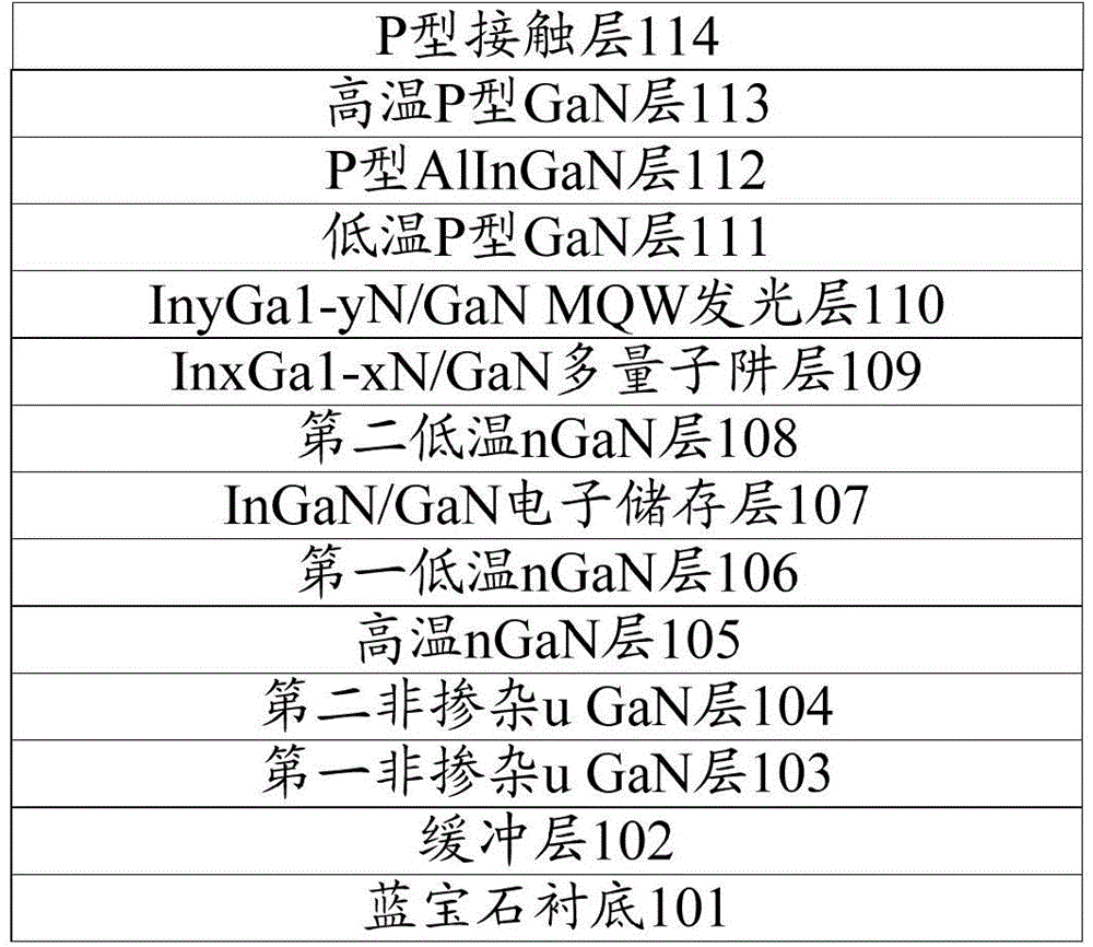
[0048] In order to improve the internal quantum efficiency of the quantum well, improve the luminous efficiency of the LED device, increase the light reflectivity and reduce the total reflection of light, the present invention provides a GAN-based green LED epitaxial structure, the structure diagram is as follows figure 1 As shown, the LED epitaxial structure includes from bottom to top: sapphire substrate 101, buffer layer 102, first undoped uGaN layer 103, second undoped uGaN layer 104, high temperature nGaN layer 105, first Low-temperature nGaN layer 106, InGaN / GaN electron storage layer 107, second low-temperature nGaN layer 108, InxGa1-xN / GaN multiple quantum well layer 109, InyGa1-yN / GaN MQW light-emitting layer 110, low-temperature P-type GaN layer 111, P-type AlInGaN layer 112, high temperature P-type GaN layer 113 and P-type contact layer 114, wherein,

[0049] The InxGa1-xN / GaN multi-quantum well layer 109 includes periodically grown InxGa1-xN / GaN well layers and Inx...

Embodiment 2

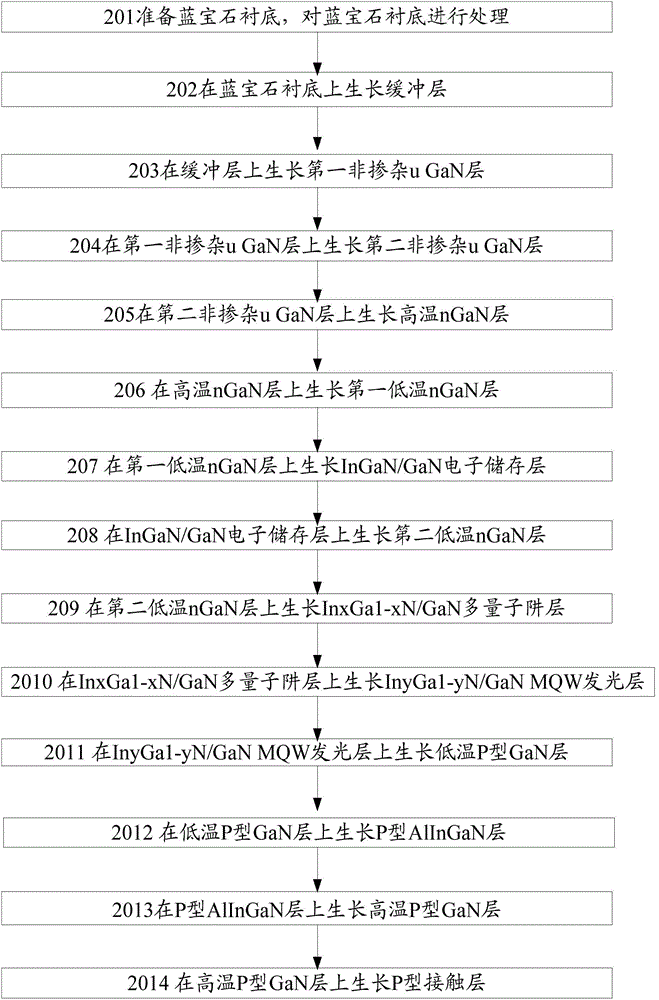
[0080] The manufacturing method of the GAN-based green LED epitaxial structure in this embodiment is carried out on Veeco K465iMOCVD equipment, and the specific process is as follows:

[0081] 1) Place the sapphire substrate in the MOCVD reaction chamber, and use H 2 , NH 3 Wait for the gas to treat the sapphire substrate at high temperature for 5-10 minutes;

[0082] 2) After the high temperature treatment is completed, the temperature in the reaction chamber is lowered to 500-600°C, the optimum temperature is 550°C, and TMGa (trimethylgallium) and NH 3 , the pressure is controlled at 300torr-650torr, and a buffer layer GaN (Nucleation) with a thickness of 15-40nm is grown on the sapphire substrate; 500s, forming a GaN crystal nucleus on the sapphire substrate;

[0083] 3) After the high temperature annealing is completed, the temperature is adjusted to 1000-1100°C, and TMGa and NH 3 , the pressure is controlled at 300torr-700torr, and the first non-doped uGaN layer with ...


PUM

PropertyMeasurementUnit
Thicknessaaaaaaaaaa
Thicknessaaaaaaaaaa
Thicknessaaaaaaaaaa

Abstract

The invention discloses GaN-based green light LED (light-emitting diode) epitaxial structure. The GaN-based green light LED epitaxial structure comprises a sapphire substrate, a buffer layer, a first undoped u GaN layer, a second undoped u GaN layer, a high-temperature nGaN layer, a first low-temperature nGaN layer, an InGaN / GaN electronic storage layer, a second low-temperature nGaN layer, an InxGal-xN / GaN multiple-quantum well layer, an InyGal-yN / GaNMQW luminescent layer, a low-temperature P type GaN layer, a P type AlInGaN layer, a high temperature P type GaN layer and a P type contact layer from bottom to top in sequence. The invention further provides a manufacturing method of the GaN-based green light LED epitaxial structure. The GaN-based green light LED epitaxial structure can be used for solving the problems of greatened lattice mismatch, strengthened polarization effect and poor crystal quality in the MQW structure of the GaN-based light emitting diode, improving the internal quantum efficiency of the internal quantum well and obviously improving the luminous efficiency of the LED apparatus.

Description

technical field [0001] The present application relates to the technical field of chip manufacturing, and more specifically, to a GaN-based green LED epitaxial structure and a manufacturing method thereof. Background technique [0002] The GaN semiconductor material with wide bandgap has good chemical and thermal stability and high breakdown voltage. It is the third-generation new semiconductor material after the first-generation silicon material and the second-generation gallium arsenide material. Its ternary alloy InGaN (In X Ga 1-X The bandgap of N) is continuously adjustable from 0.7eV to 3.4eV, and the emission wavelength covers the visible and near-ultraviolet regions. GaN-based green LEDs continue to expand their market share in the LED market, with a wide range of applications, including backlight sources for computers and LED TVs, traffic lights, large indoor and outdoor billboards, and many other fields. [0003] Since the InGaN layer of the GaN-based green light...

Claims


Application Information

Patent Timeline
IPC IPC(8): H01L33/06H01L33/32H01L33/00
CPCH01L33/005H01L33/0075H01L33/06H01L33/32H01L2933/0008H01L2933/0066
Inventor 马欢田艳红牛凤娟
Owner XIANGNENG HUALEI OPTOELECTRONICS
Why Eureka
Try Eureka