Manufacturing method of chemical nickel palladium gold plating plated with thick palladium

A production method and chemical nickel technology, which are applied in liquid chemical plating, metal material coating process, coating and other directions, can solve the problems of poor soldering performance, high production cost, poor performance of coating gold wire, etc. Good wire performance and soldering performance, reducing the use of highly toxic gold salts, and reducing production costs

Inactive Publication Date: 2015-03-18
SHENZHEN SUNTAK MULTILAYER PCB
View PDF4 Cites 18 Cited by
  • Summary
  • Abstract
  • Description
  • Claims
  • Application Information

AI Technical Summary

Problems solved by technology

[0005] The object of the present invention is to provide the preparation method of the electroless nickel-palladium-gold coating of thick-plated palladium, aim to solve the thicker gold layer thickness of the chemical nickel-palladium-gold coating in the prior art, cause production cost higher, safety reduces, coating layer The problem of poor performance of gold wire and poor soldering performance

Method used


Image

  • Manufacturing method of chemical nickel palladium gold plating plated with thick palladium
  • Manufacturing method of chemical nickel palladium gold plating plated with thick palladium

Examples


Embodiment Construction

[0019] In order to make the object, technical solution and advantages of the present invention clearer, the present invention will be further described in detail below in conjunction with the accompanying drawings and embodiments. It should be understood that the specific embodiments described here are only used to explain the present invention, not to limit the present invention.

[0020] The implementation of the present invention will be described in detail below in conjunction with specific embodiments.

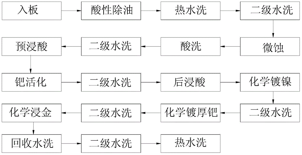
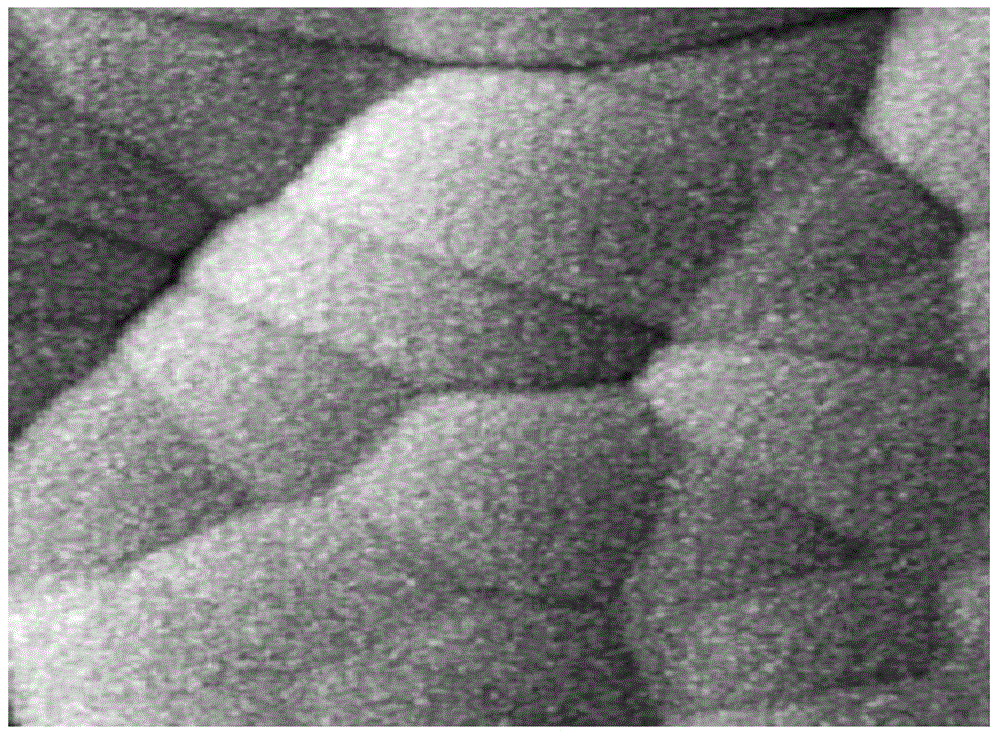
[0021] like Figure 1~2 Shown is a preferred embodiment provided by the present invention.

[0022] The preparation method of the chemical nickel-palladium-gold coating of the thick-plated palladium provided by the present embodiment is used to form a nickel-palladium-gold coating on a circuit board, and it comprises the following steps:

[0023] 1) Acid degreasing, use acid degreasing agent to clean the board surface of the circuit board, clear the oxide layer and oil ...


PUM


Abstract

The invention relates to the technical field of chemical nickel palladium gold platings, and discloses a manufacturing method of a chemical nickel palladium gold plating plated with thick palladium. The method is used for forming a nickel palladium gold plating on a surface of a circuit board, and comprises the following steps: 1) acidic oil removing; 2) micro-etching; 3) acid washing; 4) acid pre-pickling; 5) palladium activation; 6) acid post-pickling; 7) chemical nickel plating; 8) chemical plating of thick palladium, that is, chemical deposition of a palladium layer on a nickel layer of a circuit board by using organic acid and palladous sulfate; 9) chemical gold dipping. The palladium layer is formed on the nickel layer by using organic acid and palladous sulfate. The palladium layer is a palladium-storing system, and has a high thickness, so only a thin gold layer is needed to be formed on the palladium layer. Therefore, the production cost of the plating is reduced, the use of gold salt with severe toxicity is reduced, and the safety is greatly improved; figure 2 shows the surface nanometer morphology of the palladium layer; the palladium layer has low hardness and internal stress, and has excellent wetting performance; therefore, the gold wire bonding performance and the tin soldering performance of the plating are excellent.

Description

technical field [0001] The invention relates to the technical field of chemical nickel-palladium-gold plating, in particular to a method for preparing a thick palladium-plated chemical nickel-palladium-gold plating. Background technique [0002] With the gradual development of electronic products in the direction of high performance, multi-function, high reliability, light and thin, portable and low cost, in order to meet the needs of the market and technology, not only the PCB products must be moved to higher density product types, but also the electronic The packaging industry must move towards high-density packaging such as IC packaging or system packaging, which requires a coating that can meet a variety of packaging processes, so ENEPIG, a surface treatment process with a reputation of "universal" coating It came into being. [0003] The electroless nickel palladium gold process is divided into three steps, namely electroless nickel plating, electroless palladium plati...

Claims


Application Information

Patent Timeline
Patent Type & Authority Applications(China)
IPC IPC(8): C23C18/18C23C18/42C23C18/36
CPCC23C18/2073C23C18/30C23C18/36C23C18/42
Inventor 郑莎宋建远鲁惠王海民
Owner SHENZHEN SUNTAK MULTILAYER PCB
Why Eureka
Try Eureka