Full waveband infrared focal plane array based on MEMS technology

An infrared focal plane, full-band technology, applied in microstructure technology, technology for producing decorative surface effects, decorative arts, etc., can solve the problems of reduced detector sensitivity, loss of infrared energy, etc., to improve the absorption rate of infrared energy , the effect of improving sensitivity

Inactive Publication Date: 2015-03-25
PEKING UNIV
View PDF6 Cites 29 Cited by
  • Summary
  • Abstract
  • Description
  • Claims
  • Application Information

AI Technical Summary

Problems solved by technology

Infrared focal plane array where infrared radiation is incident through the substrate surface. First, the substrate will lose part of the infrared energy, which will reduce the sensitivity of the detector.
In addition, the current micro-cantilever focal plane array uses a thin dielectric layer or metal layer as the infrared absorption layer, and works in the long-wave infrared band of 8-14 μm, and cannot perform selective detection of other bands.

Method used


Image

  • Full waveband infrared focal plane array based on MEMS technology
  • Full waveband infrared focal plane array based on MEMS technology
  • Full waveband infrared focal plane array based on MEMS technology

Examples


Embodiment Construction

[0040] In order to make the object, technical solution and advantages of the present invention clearer, the structure and method of the present invention will be described in detail below with reference to the accompanying drawings.

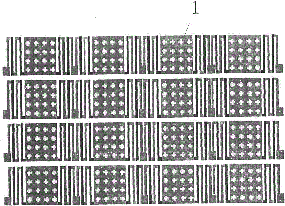
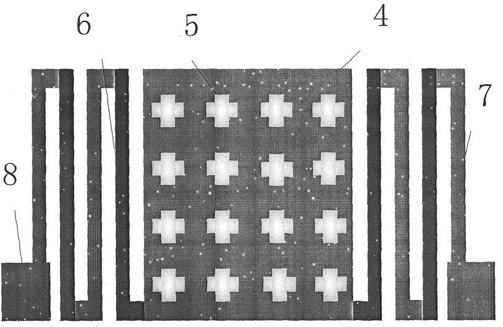
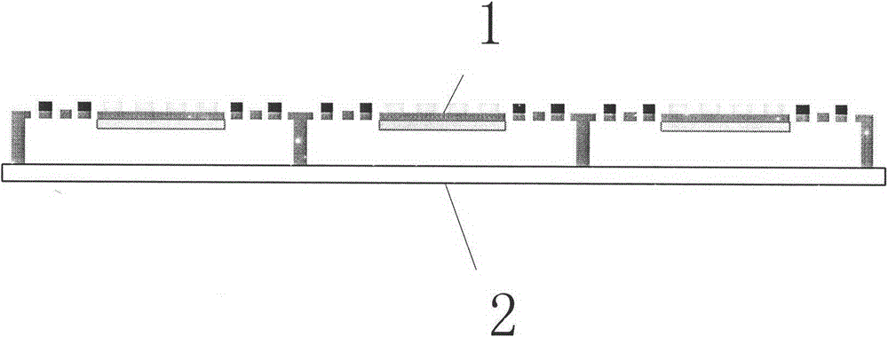
[0041] A MEMS infrared detection focal plane array, which includes a plurality of micro-cantilever beam elements (1) and a substrate (2) supporting a plurality of micro-cantilever beam elements, the substrate (2) supporting a plurality of micro-cantilever beam elements is glass , quartz sheet and other transparent materials, the substrate material has high transmittance to visible light, so that optical readout can be performed from the substrate side, so that infrared rays can directly radiate to the infrared sensitive surface without passing through the substrate, thereby improving the infrared focal plane Array sensitivity.

[0042] The number of micro-cantilever beam units (1) can be 64×64, 128×128, 256×256, 512×512 or 1024×1024, etc., and th...


PUM

PropertyMeasurementUnit
thicknessaaaaaaaaaa
thicknessaaaaaaaaaa

Abstract

The invention disclose design of a full waveband infrared focal plane array based on the MEMS technology and a manufacturing method thereof and particularly relates to the full waveband infrared focal plane array capable of realizing visible light reading from a substrate side. The full waveband infrared focal plane array comprises a transparent substrate comprising a micro cantilever pixel array and a supporting micro cantilever pixel array, a micro cantilever pixel comprises an infrared sensitive face and a micro cantilever supporting leg, and the infrared sensitive face comprises a main structure layer, an infrared absorption structure layer and an optical reflector face. When infrared light is irradiated to the focal plane array, absorbed energy is converted by the infrared absorption structure arranged on the infrared sensitive face into heat energy to make the micro cantilever pixel generate deflection, and an optical detection system reads deformation quantity and distribution of the micro cantilever pixel array through the transparent substrate. The full waveband infrared focal plane array can carry out full waveband infrared detection and imaging through employing the meta-material structure arranged on the infrared sensitive face, under the non-refrigeration work environment, the simple polyimide sacrificial layer technology can be utilized for manufacturing.

Description

technical field [0001] The invention belongs to the technical field of infrared detection and microelectromechanical systems, and relates to a design and preparation method of an infrared focal plane array, in particular to a design and preparation method of a full-band infrared focal plane array based on a transparent substrate of MEMS technology. Background technique [0002] An infrared detector is a device that detects infrared radiation from a target and converts the infrared radiation into a detectable quantity. In the civilian field, infrared thermal imaging systems can be used to manufacture automotive night vision devices and perform non-destructive testing; in the military field, it can break through the barriers of night, implement night operations, and greatly improve the combat capabilities of weapon systems. Modern infrared detection technology began to appear during World War II. The combination of photon technology and semiconductor material technology, as we...

Claims


Application Information

Patent Timeline
Patent Type & Authority Applications(China)
IPC IPC(8): G01J5/38B81B7/00B81C1/00
Inventor 于晓梅王舒阳马蔚文永正李淑玉
Owner PEKING UNIV
Why Eureka
Try Eureka