Transistor laser, and manufacturing method thereof

A technology for transistor lasers and manufacturing methods, which is applied to semiconductor lasers, lasers, laser components, etc., can solve problems such as carrier non-radiative recombination, device performance fluctuations, and material quality degradation in active regions, so as to reduce non-radiative recombination , the effect of improving device performance

Active Publication Date: 2015-04-01
INST OF SEMICONDUCTORS - CHINESE ACAD OF SCI
View PDF4 Cites 11 Cited by
  • Summary
  • Abstract
  • Description
  • Claims
  • Application Information

AI Technical Summary

Problems solved by technology

[0003] In the reported shallow ridge transistor laser structure, the quantum well active region is placed in the base region. For NPN devices, this structure has an obvious disadvantage: when using Zn, which can linearly control the hole concentration, as When p-type impurity is doped, Zn is easy to diffuse into the active region from the upper and lower directions, resulting in a significant decline in the quality of the material in the active region and deteriorating the luminous performance of the device [J.Appl.Phys., Vol 103, P.114505( 2008)]
In the reported deep ridge transistor laser [Optics Letters, Vol 36 P.3206(2011)], the quantum well active layer is placed above the base layer, thus avoiding the diffusion of Zn from above to the quantum well. However, the active layer and base layer materials of InP-based deep ridge transistor lasers are InGaAsP or InGaAlAs, which brings difficulties to the manufacture of device emitter waveguides, and the height of the waveguide can only be etched by dry or wet methods. Time control, there is a large error, resulting in fluctuations in device performance
In addition, the sidewall of the quantum well active region of the deep ridge transistor laser is exposed, and a large number of dangling bonds and other defects lead to serious non-radiative recombination of carriers, which significantly deteriorates the performance of laser devices using the deep ridge waveguide structure.

Method used


Image

  • Transistor laser, and manufacturing method thereof
  • Transistor laser, and manufacturing method thereof
  • Transistor laser, and manufacturing method thereof

Examples


Embodiment Construction

[0024] In order to make the object, technical solution and advantages of the present invention clearer, the present invention will be further described in detail below in conjunction with specific embodiments and with reference to the accompanying drawings.

[0025] see Figure 1 to Figure 6 As shown, taking an InP-based device as an example, the present invention provides a method for manufacturing a transistor laser, comprising the following steps:

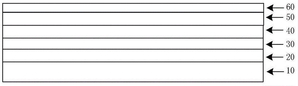
[0026] Step 1, select the substrate 10; the substrate can be an InP substrate, or a GaAs substrate, or a GaN substrate, or a SiC substrate, or a Si substrate;

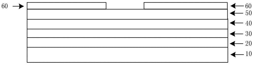
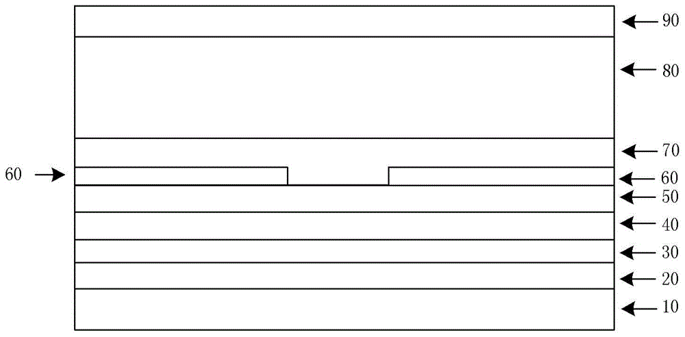
[0027] Step 2, growing a buffer layer 20, a lower collector layer 30, a collector layer 40, a base layer 50 and a current blocking layer 60 sequentially on the upper surface of the substrate 10, such as figure 1 shown.

[0028] The material of the base layer 50 is InGaAsP material. The current blocking layer 60 is In x Ga 1-x P material (where 0≤x≤1). The current ...


PUM


Abstract

The invention discloses a transistor laser, and a manufacturing method thereof. The method includes the following steps: a substrate is selected; a buffer layer, a lower collector layer, a collector layer, a base layer and a current blocking layer are grown in sequence; part of current blocking layer materials are selectively etched; an active layer, an emitter layer and a contact layer are grown; an emitter ridge waveguide is etched until reaching the current blocking layer; the current blocking layer between base layer materials of the device and active layer materials of the device can serve as an emitter waveguide etching stop layer, so as to achieve high-precision control of the waveguide height. The current blocking layer materials below the emitter ridge waveguide are selectively etched, so as to limit lateral diffusion of carriers, and help reduce non-radiative recombination of the carriers on the side wall of an active area. These measures can remarkably improve the performances of the device.

Description

technical field [0001] The invention relates to the field of semiconductor optoelectronic devices, in particular to a transistor laser and a manufacturing method thereof. Background technique [0002] In 2005, a research team from the University of Illinois in the United States first reported a semiconductor device called a heterojunction bipolar transistor laser in the world [Appl.Phys.Lett.Vol.87, P.131103 (2005) .], only using a relatively simple epitaxy and manufacturing process, the device simultaneously realizes the light emitting function of the laser and the amplification function of the transistor. The difference from ordinary transistors is that a quantum well is introduced in the base region of the transistor. Under a certain base-collector voltage, electrons will be injected into the base region from the collector region, and recombine with holes in the quantum well region to emit light. The light wave is reflected back and forth between the front and rear two ...

Claims


Application Information

Patent Timeline
Patent Type & Authority Applications(China)
IPC IPC(8): H01S5/34H01S5/343
Inventor 梁松朱洪亮
Owner INST OF SEMICONDUCTORS - CHINESE ACAD OF SCI
Why Eureka
Try Eureka