Method for welding silicon wafer and molybdenum piece in semiconductor device and application of silicon wafer and molybdenum piece

A semiconductor and silicon wafer technology, applied in semiconductor devices, semiconductor/solid-state device manufacturing, electrical solid-state devices, etc., can solve the problems of large ohmic contact between silicon wafers and molybdenum wafers, reduced ohmic contact effect, and reduced component life, etc., to improve The effect of anti-surge current ability and firmness, small contact thermal resistance and transient thermal impedance, good thermal conductivity and electrical conductivity

Active Publication Date: 2015-04-22
ZHUZHOU CRRC TIMES SEMICON CO LTD
View PDF4 Cites 5 Cited by
  • Summary
  • Abstract
  • Description
  • Claims
  • Application Information

AI Technical Summary

Problems solved by technology

The traditional sintering process is only suitable for the welding of silicon wafers and molybdenum wafers below 4 inches; 2) Due to the phenomenon of large deformation in the sintering process, the long-term reliability of the components is poor
The service life of components is greatly reduced; 3) Sintering is a brazing process, which is carried out at high temperature, which easily leads to the formation of thermal stress bubbles, resulting in poor stickiness and large void rate; 4) Sintering process has poor stickiness , resulting in a larger ohmic contact between the silicon wafer and the molybdenum wafer, resulting in a larger contact pressure drop of the final component; 5) poor thermal contact between the silicon wafer and the molybdenum wafer due to poor sintering process, resulting in poor component The contact thermal resistance and transient thermal resistance are relatively large; 6) Due to the high temperature of the sintering process, the surface of the silicon wafer is easy to grow an oxide layer
This layer of oxide layer prevents direct contact between the silicon wafer and the alloy material, and it is difficult for the two to fuse, resulting in a decrease in the ohmic contact effect.

Method used


Image

  • Method for welding silicon wafer and molybdenum piece in semiconductor device and application of silicon wafer and molybdenum piece
  • Method for welding silicon wafer and molybdenum piece in semiconductor device and application of silicon wafer and molybdenum piece
  • Method for welding silicon wafer and molybdenum piece in semiconductor device and application of silicon wafer and molybdenum piece

Examples


Embodiment 1

[0047] A method comprising the following steps is adopted to prepare a soldered product of a silicon wafer / molybdenum wafer in a semiconductor device:

[0048] a. Sputter silver on one side of the molybdenum sheet, and the thickness of the first silver layer obtained by sputtering is 0.5 μm;

[0049] b. Sputtering titanium, nickel and silver sequentially on the anode surface of the silicon wafer. The thicknesses of the obtained titanium layer, nickel layer and second silver layer are successively 0.1 μm, 0.5 μm and 1 μm;

[0050] c. Transfer nano-silver to the first silver layer under the process conditions of 150°C and 0.3MPa, and remove the supporting material polytetrafluoroethylene film of the nano-silver layer, and then contact the second silver layer;

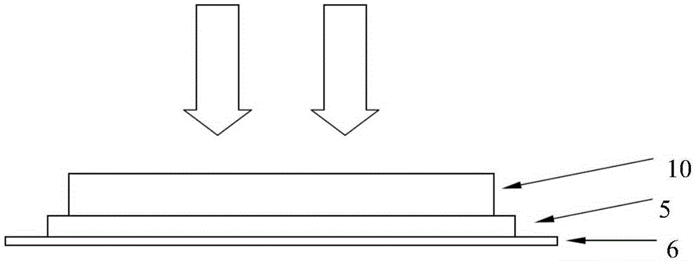
[0051] d. Under the process conditions of 250°C and 15MPa, the welding is realized, the process time is about 2 minutes, and then slowly cooled by natural cooling. Graphite is used as a buffer layer on the cathode side ...

Embodiment 2

[0054] A method comprising the following steps is adopted to prepare a soldered product of a silicon wafer / molybdenum wafer in a semiconductor device:

[0055] a. Sputter silver on one side of the molybdenum sheet, and the thickness of the first silver layer obtained by sputtering is 0.4 μm;

[0056] b. Sputtering titanium, nickel and silver sequentially on the anode surface of the silicon wafer. The thicknesses of the obtained titanium layer, nickel layer and second silver layer are successively 0.2 μm, 0.5 μm and 1.1 μm;

[0057] c. Transfer nano-silver to the first silver layer under the process conditions of 150°C and 0.3MPa, and remove the supporting material polytetrafluoroethylene film of the nano-silver layer, and then contact the second silver layer;

[0058] d. Under the process conditions of 300°C and 15MPa, the welding is realized, the process time is about 2 minutes, and then slowly cooled by natural cooling. Graphite is used as a buffer layer on the cathode sid...

Embodiment 3

[0061] A method comprising the following steps is adopted to prepare a soldered product of a silicon wafer / molybdenum wafer in a semiconductor device:

[0062] a. Sputter silver on one side of the molybdenum sheet, and the thickness of the first silver layer obtained by sputtering is 0.5 μm;

[0063] b. Sputtering titanium, nickel and silver sequentially on the anode surface of the silicon wafer. The thicknesses of the obtained titanium layer, nickel layer and second silver layer are successively 0.1 μm, 0.5 μm and 1 μm;

[0064] c. Transfer nano-silver to the first silver layer under the process conditions of 150°C and 0.3MPa, and remove the supporting material polytetrafluoroethylene film of the nano-silver layer, and then contact the second silver layer;

[0065] d. Under the process conditions of 250°C and 10MPa, welding is realized, the process time is about 2 minutes, and then slowly cooled by natural cooling. Graphite is used as a buffer layer on the cathode side of t...


PUM

PropertyMeasurementUnit
thicknessaaaaaaaaaa
thicknessaaaaaaaaaa
thicknessaaaaaaaaaa

Abstract

The invention discloses a method for welding a silicon wafer and a molybdenum piece in a semiconductor device. The method comprises the following steps that firstly, a first silver layer is arranged on the molybdenum piece; secondly, a second silver layer is arranged on the anode electrode of the silicon wafer; thirdly, a third silver layer is arranged between the first silver layer and the second silver layer; fourthly, the silicon wafer and the molybdenum piece are welded together by welding the first silver layer, the second silver layer and the third silver layer. According to the method, the technology is simple, the yield and the welding strength are high, the voidage of welding layers is low, the deformation is small, and the performance of the product can be greatly improved. The invention further relates to an application of the silicon wafer/molybdenum piece manufactured through the method.

Description

technical field [0001] The invention relates to the field of semiconductors, and relates to a method for welding a silicon chip and a molybdenum chip in a semiconductor device. The present invention also relates to the application of the silicon wafer / molybdenum wafer welding product prepared by the above method. Background technique [0002] After the semiconductor chip is processed by multiple processes such as diffusion, photolithography and mesa molding, the chip has certain electrical characteristics. But the chip cannot be used directly, because the chip itself is very fragile, it is easily damaged by collision, and it cannot be powered on. Therefore, a molybdenum sheet is often welded to the silicon chip. On the one hand, it can protect the silicon chip from being damaged by collision, so that it cannot be used any longer; The purpose of welding has two aspects: one is to make the anode surface of the chip form a good ohmic contact and thermal contact with the metal...

Claims


Application Information

Patent Timeline
Patent Type & Authority Applications(China)
IPC IPC(8): H01L21/60
CPCH01L24/03H01L2224/02125H01L2224/0333H01L2924/01047
Inventor 朱为为吴煜东颜骥张明邹冰艳操国宏唐革王政英姚震洋刘芹高军
Owner ZHUZHOU CRRC TIMES SEMICON CO LTD
Why Eureka
Try Eureka