
High-brightness near ultraviolet LED and preparation method thereof
A near-ultraviolet, high-brightness technology, used in semiconductor devices, electrical components, circuits, etc., can solve problems such as affecting luminous efficiency, unable to eliminate V-type dislocations, increasing quantum well and barrier layer stress mismatch, etc., to improve luminescence. Efficiency, effect of improving current spreading effect
- Summary
- Abstract
- Description
- Claims
- Application Information
AI Technical Summary
Problems solved by technology
Method used
Image

Examples
Embodiment 1
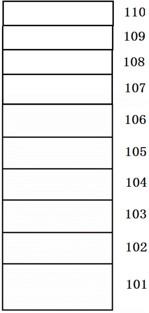
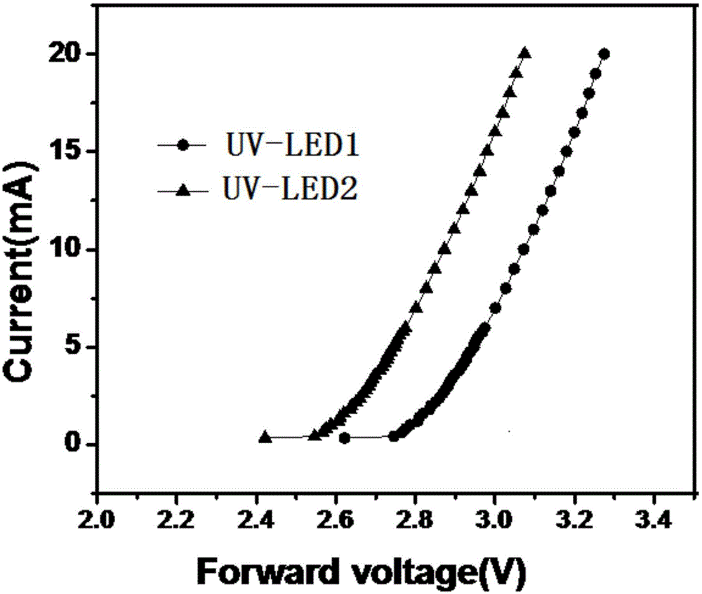
[0020] Use Aixtron company, tightly coupled vertical reaction chamber MOCVD growth system. Trimethylgallium (TMGa), trimethylindium (TMIn), trimethylaluminum (TMAl) were used as Group III sources during the growth process, ammonia (NH 3 ) as a Group V source, silane (SiH 4 ) as an n-type dopant source, dimagnesocene (Cp 2 Mg) as a p-type dopant source, the patterned Al 2 o 3 The substrate 101 is heated to 1080-1100 degrees centigrade, and the pressure in the reaction chamber is 100 torr. 2 Under treatment for 5 minutes, then cool down to 530-550 degrees Celsius in the patterned Al 2 o 3On the substrate, the pressure of the reaction chamber is 500torr, under the hydrogen (H2) atmosphere, the V / III molar ratio is 500-1300, and the GaN nucleation layer after three-dimensional growth of 20-30 nanometers, at 1000-1500°C, the reaction chamber pressure is 200-300torr, in hydrogen (H 2 ) atmosphere, the V / III molar ratio is 1000-1300; grow a 1-3 micron thick high-temperature u-...
Embodiment 2
[0022] Use Aixtron company, tightly coupled vertical reaction chamber MOCVD growth system. Trimethylgallium (TMGa), trimethylindium (TMIn), trimethylaluminum (TMAl) were used as Group III sources during the growth process, ammonia (NH 3 ) as a Group V source, silane (SiH 4 ) as an n-type dopant source, dimagnesocene (Cp 2 Mg) as a p-type dopant source, the patterned Al 2 o 3 The substrate is heated to 1080-1100 degrees Celsius, the pressure in the reaction chamber is 100torr, and the H 2 Under treatment for 5 minutes, then cool down to 530-550 degrees Celsius in the patterned Al 2 o 3 On the substrate, the pressure of the reaction chamber is 500torr, under the hydrogen (H2) atmosphere, the V / III molar ratio is 500-1300, and the GaN nucleation layer after three-dimensional growth of 20-30 nanometers, at 1000-1500°C, the reaction chamber pressure is 200-300torr, in hydrogen (H 2 ) atmosphere, the V / III molar ratio is 1000-1300; grow a 1-3 micron thick high-temperature u-G...
PUM
 Abstract
Description
Claims
Application Information