Preparation method for printing independent carbon nano tube thin film transistor in large area

A carbon nanotube thin film, thin film transistor technology, applied in nanotechnology, nanotechnology, semiconductor/solid-state device manufacturing, etc., to achieve the effects of environmental friendliness, superior electrical performance, and low cost

Active Publication Date: 2015-04-29
SUZHOU INST OF NANO TECH & NANO BIONICS CHINESE ACEDEMY OF SCI
View PDF3 Cites 15 Cited by
  • Summary
  • Abstract
  • Description
  • Claims
  • Application Information

AI Technical Summary

Problems solved by technology

However, through the investigation of the domestic research status, it is not difficult to find that domestic research in this field is mainly carried out in the field of organic materials, and in the field of chemistry. Compared with foreign countries, the research on the use of printing technology to prepare large-area electronic devices big gap

Method used


Image

  • Preparation method for printing independent carbon nano tube thin film transistor in large area
  • Preparation method for printing independent carbon nano tube thin film transistor in large area
  • Preparation method for printing independent carbon nano tube thin film transistor in large area

Examples


Embodiment 1

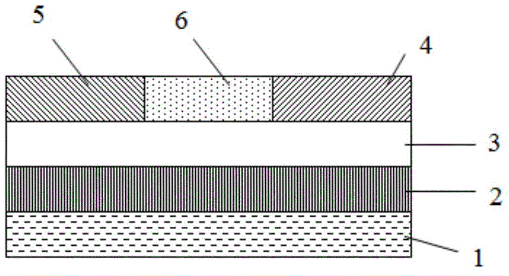
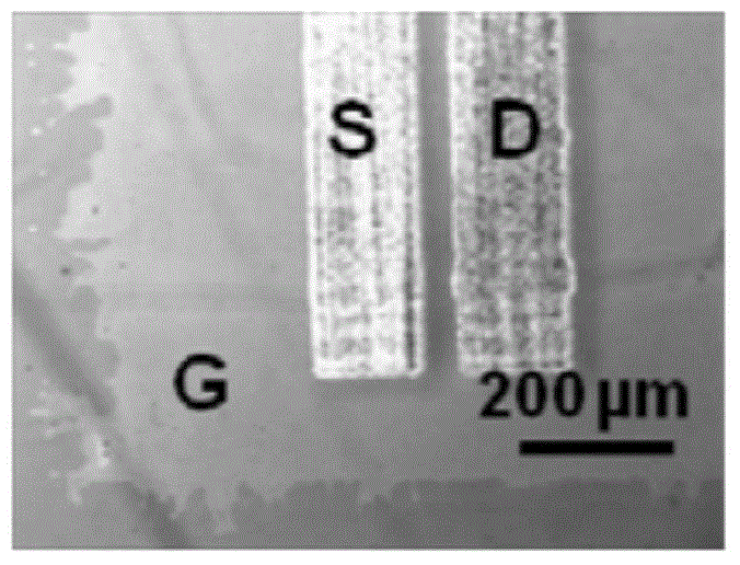
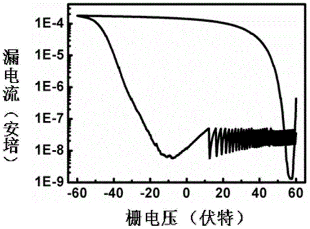
[0029] After the glass substrate is cleaned, it is blown dry with nitrogen or air. First, a large-area ITO electrode array is printed on the glass substrate by aerosol inkjet printing. After drying, in order to make the ITO electrode conductive, the printed ITO electrode is placed on the Anneal in the air at 500°C for 30 minutes; then deposit a layer of aluminum oxide dielectric layer on the surface of the ITO electrode by atomic layer deposition, and then print a pair of ITO source and drain on the top of the ITO electrode by aerosol inkjet printing A 200-micron-wide channel is formed between the source electrode and the drain electrode, and the ITO source and drain electrodes are placed in the air and annealed at 500 ° C for 30 minutes, and then ultrasonicated in ethanol, acetone and pure water respectively. Dry it for 5 minutes; finally soak the whole glass substrate in the toluene solution of P3DDT-P2 for 6 to 12 hours, take out the electrodes, rinse them twice with toluene...

Embodiment 2

[0032]Select a flexible polymer substrate such as a PI substrate (which can withstand high temperatures of 280 degrees), clean it and blow it dry with nitrogen or air. First, use aerosol inkjet printing to print a large-area silver electrode array on the PI substrate. After drying, in order to make The silver electrode conducts electricity, and the printed silver electrode is placed in the air and annealed at 200°C for 30 minutes; then a layer of hafnium oxide is deposited on the surface of the silver electrode by atomic layer deposition, and then printed on the silver electrode by aerosol inkjet printing. Print a pair of silver source and drain electrodes on the top of the electrode, and form a 150 micron wide channel between the source and drain electrodes, and place the silver source and drain electrodes in air and anneal at 200°C for 30 minutes; finally put The entire flexible PI substrate was soaked in the toluene solution of PFO-CG200 for 6-12 hours, then the electrodes w...

Embodiment 3

[0034] Select a flexible polymer substrate such as a PET substrate, clean it and blow it dry with nitrogen or air. First, use the transfer printing method aerosol inkjet printing to print a large-area silver electrode array on the PET substrate. After drying, in order to make the silver electrode conductive , place the printed silver electrode in air and anneal at 200°C for 30 minutes; then deposit a layer of aluminum oxide on the surface of the silver electrode by atomic layer deposition, and then print on the silver electrode by aerosol inkjet printing A pair of silver source and drain electrodes, a 100 micron wide channel is formed between the source electrode and the drain electrode, and the silver source and drain electrodes are placed in the air and annealed at 200°C for 30 minutes; finally the entire glass sheet Soak in the m-xylene solution of F8T2-P2 for 6 to 12 hours, take out the electrode, wash it twice with m-xylene, and measure the electrical properties. The mobi...


PUM

PropertyMeasurementUnit
areaaaaaaaaaaa
diameteraaaaaaaaaa
widthaaaaaaaaaa

Abstract

The invention discloses a preparation method for printing an independent carbon nano tube thin film transistor in a large area. The preparation method comprises the following steps: (a) providing a substrate; (b) preparing a gate electrode array on the substrate by a printing technology; (c) preparing a dielectric layer on the gate electrode array by an atomic deposition technology, a spin coating technology or the printing technology; (d1) firstly preparing a source electrode and a drain electrode on the dielectric layer by the printing technology, wherein a trench which is 10-200 microns in width is formed between the source electrode and the drain electrode; then preparing a carbon nano tube active layer in the trench by the printing technology; or (d2) preparing the carbon nano tube active layer which is 10-200 microns in width on the dielectric layer by the printing technology, and then respectively preparing the source electrode and the drain electrode on the two sides of the active layer. The preparation method provided by the invention is simple in technology, environmental-friendly, convenient to operate and low in cost.

Description

technical field [0001] The invention relates to a method for preparing a thin film transistor, in particular to a method for preparing a large-area printed independent carbon nanotube thin film transistor in the field of printed nanoelectronics, and belongs to the field of printed nanoelectronics. Background technique [0002] Printed electronics technology is an emerging technology and industry field that has only flourished in the world in the past five years. According to experts' prediction, the total value of printed electronics products in the world will reach 330 billion US dollars in 2017. Therefore, the development of printed electronics technology has been favored by people all over the world. It has become a multidisciplinary and comprehensive cutting-edge research hotspot. Although the performance of printed electronic devices is not as good as that of silicon-based semiconductor microelectronic devices, due to its simple printing process and non-selectivity to s...

Claims


Application Information

Patent Timeline
Patent Type & Authority Applications(China)
IPC IPC(8): H01L21/336B82Y10/00
Inventor 赵建文徐文亚王超钱龙张建辉崔铮
Owner SUZHOU INST OF NANO TECH & NANO BIONICS CHINESE ACEDEMY OF SCI
Why Eureka
Try Eureka