A post-processing method for solar cells

A technology of solar cells and silicon wafers, applied in circuits, photovoltaic power generation, electrical components, etc., to achieve the effects of improving uniformity and compactness, improving resistance to hidden cracks, and enhancing competitiveness

Active Publication Date: 2017-04-26
山东力诺阳光电力科技有限公司
View PDF5 Cites 4 Cited by
  • Summary
  • Abstract
  • Description
  • Claims
  • Application Information

AI Technical Summary

Problems solved by technology

But in the final analysis, the self-strength of photovoltaic modules still needs to be improved

Method used


Image

  • A post-processing method for solar cells
  • A post-processing method for solar cells

Examples


Embodiment 1

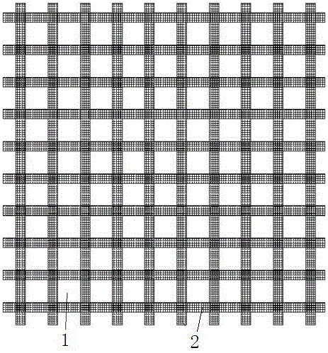
[0025] Select polysilicon wafer; 1) Surface structuring of silicon wafer, making emitter, peripheral etching, removal of phosphosilicate glass, silicon nitride film, silk screen front and back electrodes and back aluminum, sintering; 2) The battery obtained in step 1 Make a layer of non-stick coating with a thickness of 20 microns on the back of the sheet aluminum, and the non-stick coating is polytetrafluoroethylene resin; 3) Put the battery sheet obtained in step 2 into an annealing furnace, and pass in hydrogen gas , keep the temperature at 300°C for 220s. The non-stick coating is hollowed out with a grid structure, as shown in the attached picture of the instruction manual figure 1 As shown, the hollowed out area 1 is a square, the width of the grid structure hollowed out area 1 is 0.8 mm, and the width of the grid structure non-hollowed out area 2 is 1 mm.

Embodiment 2

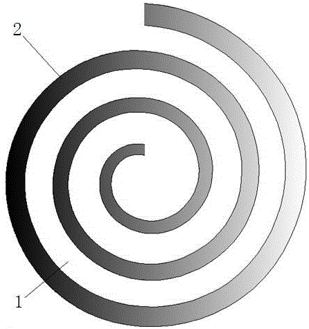
[0027] Select a single crystal silicon wafer; 1) Process the silicon wafer through surface structuring, making emitters, peripheral etching, removal of phosphosilicate glass, silicon nitride film, silk screen front and back electrodes and back aluminum, and sintering; 2) Step 1 Make a layer of non-stick coating with a thickness of 30 microns on the aluminum back field of the obtained battery sheet, and the non-stick coating is polyimide resin; 3) Put the battery sheet obtained in step 2 into an annealing furnace, pass through Hydrogen gas, keep the temperature at 200°C for 500s. The non-stick coating is hollowed out with a spiral structure, the average width of the hollowed out area 1 of the spiral structure is 2mm, and the average width of the non-hollowed out area 2 of the spiral structure is 2mm.

Embodiment 3

[0029] Select a single crystal silicon wafer; 1) Process the silicon wafer through surface structuring, making emitters, peripheral etching, removal of phosphosilicate glass, silicon nitride film, silk screen front and back electrodes and back aluminum, and sintering; 2) Step 1 A layer of non-stick coating with a thickness of 50 microns is made on the aluminum back field of the obtained cell, and the non-stick coating is silicone oil; 3) The cell obtained in step 2 is put into an annealing furnace, and hydrogen gas is introduced to keep The temperature is 260°C, and the time is 400s. The non-stick coating is hollowed out with a grid structure, as shown in the attached picture of the instruction manual figure 1 As shown, the hollowed-out area 1 is elliptical, the average width of the grid-structured hollowed-out area 1 is 1.5mm, and the average width of the grid-structured non-hollowed-out area 2 is 3mm.


PUM

PropertyMeasurementUnit
thicknessaaaaaaaaaa
thicknessaaaaaaaaaa
thicknessaaaaaaaaaa

Abstract

The invention relates to a post-processing method of a solar cell piece. The post-processing method adopts a non-stick coating to greatly improve the anti-subfissure capability of the solar cell piece and a subsequent solar assembly; the low-temperature sintering process can be used for drying the non-stick coating and further effectively repairing the microdefect in the cell piece; meanwhile, the uniformity and the compactness of the silicon nitride thin film can be effectively improved; the passivation effect of the silicon nitride thin film can be improved, so that the service life of a minority carrier of the cell piece can be prolonged; in addition, the PID resistance of the high-temperature annealed cell piece can be improved. Therefore, the post-processing method is significant in production practical value, and can improve the competitiveness for an enterprise.

Description

technical field [0001] The invention relates to the technical field of solar cell production, in particular to a post-processing method for solar cell sheets. Background technique [0002] With the continuous development of the crystalline silicon solar energy market, more and more quality problems have been exposed, and the industry's understanding of the quality of photovoltaic cell modules has become more and more in-depth. At present, more attention is being paid to micro-cracks in photovoltaic modules, that is, cracks appear in solar cells packaged in photovoltaic modules. Due to the existence of the package and the viscosity of EVA, the fragments of the split battery parts still maintain the original combination and conduction. There is not much change in the appearance and output power in a short time, which can only be measured with an electroluminescence tester (EL). However, in the long run, there is a hidden danger that the thermal expansion and contraction betw...

Claims


Application Information

Patent Timeline
Patent Type & Authority Patents(China)
IPC IPC(8): H01L31/18
CPCH01L31/186Y02E10/50Y02P70/50
Inventor 任现坤王光利尹兰超黄国强姜言森贾河顺马继磊张春艳徐振华支开印陈兵兵
Owner 山东力诺阳光电力科技有限公司
Why Eureka
Try Eureka