Method for preparing nano bowl-shaped phase change memory unit

A phase change memory, nano bowl technology, applied in nanotechnology, nanotechnology, nanotechnology for information processing, etc., to achieve the effects of reducing energy loss, reducing the range of heat diffusion, and increasing current density

CN104576925AActive Publication Date: 2015-04-29JILIN NORMAL UNIV
5 Cites 3 Cited by

Patent Information

Authority / Receiving Office
CN · China
Patent Type
Applications(China)
Current Assignee / Owner
Publication Date
2015-04-29

Smart Images

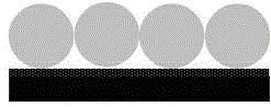
  • Figure 1
    Figure 1
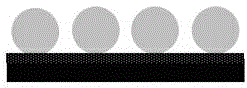
  • Figure 2
    Figure 2
  • Figure 3
    Figure 3
Patent Text Reader

Abstract

The invention relates to a method for preparing a nano structure material for a novel semiconductor memory, in particular relates to a method for preparing a nano bowl-shaped phase change memory unit, and aims to prepare a nano bowl array and a nano bowl-shaped top electrode made of a phase change material such as GeSbTe or GeTe by taking a nano colloidal sphere array in a two-dimensional order. By adopting the hollow nano bowl-shaped phase change memory unit, the loss of heat from the electrode in the amorphous to polycrystal conversion process of the phase change material is reduced, the contact area of the phase change material with a lower electrode is reduced, the current density is improved, and the operation current of a device is reduced.
Need to check novelty before this filing date? Find Prior Art

Description

technical field

[0001] The invention relates to a preparation method of a nanostructure material applicable to novel semiconductor storage, in particular to a preparation method of a nanobowl-shaped phase-change memory unit. Background technique

[0002] Phase change random access memory (PCM) uses the resistance of the crystalline and amorphous states of chalcogenide compounds (such as GeSbTe or GeTe, etc.) to realize data storage. Phase change memory has the advantages of non-volatility, long cycle life, small device size, high speed, radiation resistance, and multi-level storage.

[0003] Phase change memory is composed of many phase change memory cells. Each phase-change memory cell includes three basic parts: top electrode, phase-change medium, and bottom electrode. The current phase-change memory cell preparation is realized by traditional photolithography technology, so each phase-change memory cell is made of planar composed of thin film structures. To further inc...

Examples

Embodiment Construction

[0024] ①. Put the Si or quartz substrate on the NH 4 OH (analytical pure), H 2 o 2 (analytically pure) and H 2 The mixed solution composed of O (volume ratio 1:2:6) was boiled for 5 minutes, then rinsed with deionized water and dried in an oven. On the dried Si or quartz substrate, the magnetron sputtering technology is used to grow the conductive thin film TiN or W with a thickness of 10 nm to form the bottom electrode ( figure 1 ). TiN or W thin films were prepared in a magnetron sputtering system (model ATC 1800-F, USA AJA) produced in the United States. The background pressure in the magnetron sputtering system is 1.8×10 ?6 Torr, the sputtering pressure is 2mTorr, Ar gas is used as the shielding gas, and the sputtering power is 20 watts. At this time, the sputtering rate of TiN was 0.049 nm / s (the sputtering rate of W was 0.057 nm / s).

[0025] ②. Soak the bottom electrode in step ① in a 10% sodium lauryl sulfate solution for 24 hours, so that we can get a hydrophil...