Organic electroluminescent device and preparation method thereof

An electroluminescent device and electroluminescent technology, which can be applied in the fields of electro-solid devices, semiconductor/solid-state device manufacturing, electrical components, etc., and can solve problems such as low luminous efficiency

Inactive Publication Date: 2015-04-29
OCEANS KING LIGHTING SCI&TECH CO LTD +2
View PDF0 Cites 2 Cited by
  • Summary
  • Abstract
  • Description
  • Claims
  • Application Information

AI Technical Summary

Problems solved by technology

However, the luminous efficiency of organic

Method used


Image

  • Organic electroluminescent device and preparation method thereof
  • Organic electroluminescent device and preparation method thereof
  • Organic electroluminescent device and preparation method thereof

Examples


preparation example Construction

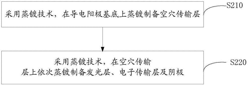
[0037] see figure 2 , the preparation method of the organic electroluminescent device of an embodiment, comprises the following steps:

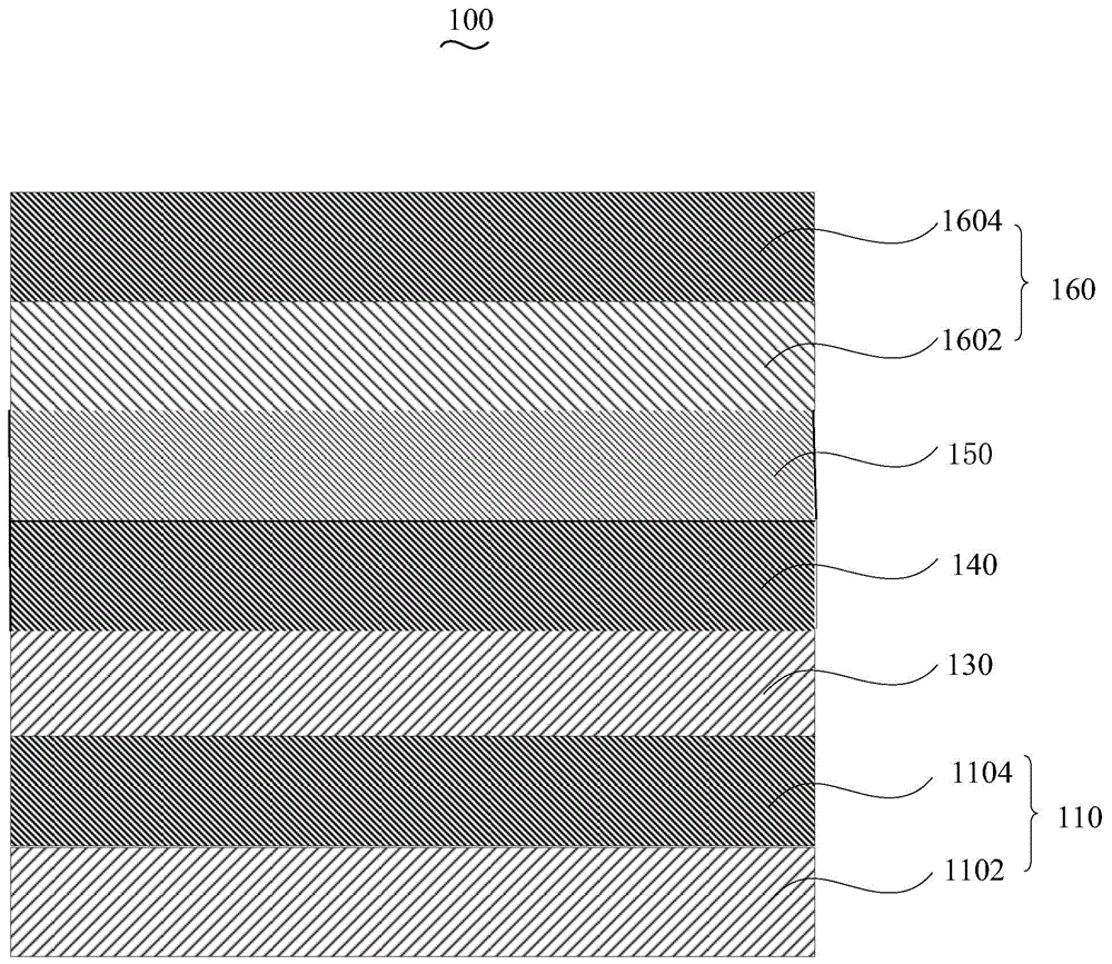
[0038] S210 , preparing a hole transport layer 130 on the conductive anode substrate 110 by evaporation using an evaporation technique.

[0039] Wherein, the conductive anode substrate 110 includes a transparent substrate 1102 and an anode layer 1104 prepared on the transparent substrate 1102 . Preferably, the transparent substrate 1102 is glass. The material of the anode layer 1104 is indium tin oxide (ITO). The sheet resistance of the anode layer 1104 is 5˜100Ω / sq.

[0040] Preferably, before the surface of the anode layer of the conductive anode substrate is vapor-deposited to prepare the hole transport layer, a step of cleaning the conductive anode substrate is also included. The cleaning step is as follows: the conductive anode substrate is ultrasonically cleaned with detergent, deionized water, acetone, ethanol and isopropanol in s...

Embodiment 1

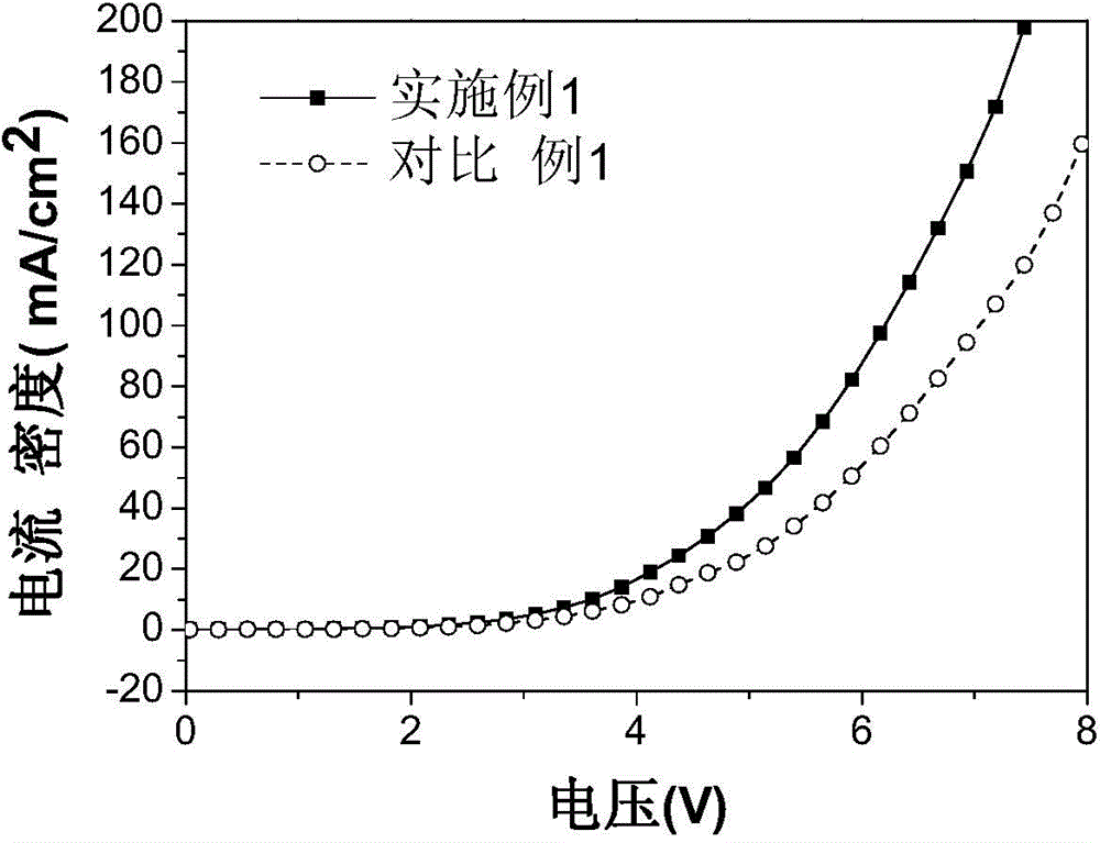
[0063] The structure of the organic electroluminescent device prepared in this embodiment is: ITO / Cu 2 O:NPB / TPBi:Ir(ppy) 3 / Bphen / LiF / Ag; where, the slash " / " indicates a layered structure, and the colon ":" indicates doping, the same below.

[0064] The preparation of the organic electroluminescent device of this embodiment is as follows:

[0065] (1) Wash the ITO glass substrate sequentially with detergent, deionized water, and ultrasonic for 15 minutes to remove organic pollutants on the glass surface. The square resistance of the ITO conductive glass is 5Ω / sq.

[0066] (2) In a vacuum of 1×10 -5 In Pa's vacuum coating system, a hole transport layer is prepared on the surface of the conductive anode ITO. The material of the hole transport layer includes organic hole transport materials and doping materials doped in organic hole transport materials. Organic hole transport materials For NPB, the doping material is Cu 2 O, Cu 2 The mass ratio of O to NPB is 5:100, the th...

Embodiment 2

[0075] The structure of the organic electroluminescent device prepared in this embodiment is: ITO / CuF:MeO-TPD / DPVBi / TPBi / CsF / Al.

[0076] The preparation of the organic electroluminescent device of this embodiment is as follows:

[0077] (1) Wash the ITO glass substrate sequentially with detergent, deionized water, and ultrasonic for 15 minutes to remove organic pollutants on the glass surface. The square resistance of the ITO conductive glass is 100Ω / sq.

[0078] (2) In a vacuum of 1×10 -4 In Pa's vacuum coating system, a hole transport layer is prepared on the surface of the conductive anode ITO. The material of the hole transport layer includes organic hole transport materials and doping materials doped in organic hole transport materials. Organic hole transport materials It is MeO-TPD, the doping material is CuF, the mass ratio of CuF to MeO-TPD is 30:100, the thickness of the hole transport layer is 100nm, and the cuprous fluoride is evaporated by electron beam, and the ...


PUM

PropertyMeasurementUnit
Thicknessaaaaaaaaaa
Thicknessaaaaaaaaaa
Thicknessaaaaaaaaaa

Abstract

The invention discloses an organic electroluminescent device. The organic electroluminescent device comprises a conductive anode substrate as well as a ,hole transport layer, a light-emitting layer, an electronic transmission layer and a cathode which are stacked on an anode layer of the conductive anode substrate in sequence, wherein the anode layer is made from indium tin oxide; materials of the hole transport layer comprise the organic hole transport material and a doping material doped in the organic hole transport material; the doping material is an oxide of copper or a fluoride of copper; the oxide of the copper is at least one of copper oxide and cuprous oxide; the fluoride of the copper is at least one of copper fluoride and cuprous fluoride; HOMO energy level of the organic hole transport layer is 5.0 eV-5.4 eV; a mass ratio of the doping material to the organic hole transport material is (5:100) to (30:100). The organic electroluminescent device is relatively high in light-emitting efficiency. The invention further provides a preparation method for the organic electroluminescent device.

Description

technical field [0001] The invention relates to the field of organic electroluminescent devices, in particular to an organic electroluminescent device and a preparation method thereof. Background technique [0002] The luminescence principle of organic electroluminescent devices is based on the action of an external electric field, electrons are injected from the cathode to the lowest unoccupied molecular orbital (LUMO) of organic matter, and holes are injected from the anode to the highest occupied molecular orbital (HOMO) of organic matter. Electrons and holes meet, recombine, and form excitons in the light-emitting layer. Excitons migrate under the action of an electric field, transfer energy to the light-emitting material, and excite electrons to transition from the ground state to the excited state. The excited state energy is deactivated by radiation to generate photons , releasing light energy. However, the luminous efficiency of organic electroluminescent devices is...

Claims


Application Information

Patent Timeline
IPC IPC(8): H01L51/52H01L51/54H01L51/56
CPCH10K71/166H10K50/155
Inventor 周明杰冯小明钟铁涛王平
Owner OCEANS KING LIGHTING SCI&TECH CO LTD
Why Eureka
Try Eureka