
Table chip double side electrophoresis glass passivation technology

A glass passivation and electrophoresis technology, applied in the manufacturing of circuits, electrical components, semiconductor/solid-state devices, etc., can solve the problems of poor electrical properties of devices, glass peeling, poor reliability, etc., and achieve improved thickness consistency and surge resistance. The effect of enhancement, voltage stability improvement

Active Publication Date: 2015-05-06
SUZHOU QILAN POWER ELECTRONICS
View PDF6 Cites 4 Cited by
  • Summary
  • Abstract
  • Description
  • Claims
  • Application Information

AI Technical Summary

Problems solved by technology

The knife scraping method has the disadvantages of uneven glass layer and poor reliability; the photoresist method has the problems of high cost and complicated process; the electrophoresis method has the advantages of simple process and high reliability and is applied to the passivation protection of mesa chips
However, the commonly used double-sided electrophoresis method is usually the process of electrophoresis on one side and then on the other side, and there are the following problems: when the second side is electrophoresed, the glass on the part of the first side that has been electrophoresed will fall off; the two electrophoresis will cause The thickness and shape of the glass layer on both sides of the device are inconsistent; the two electrophoresis operations take a long time, which affects production efficiency
Two electrophoresis processes will cause defects such as poor electrical properties, low yield and poor reliability of the device

Method used


Image

  • Table chip double side electrophoresis glass passivation technology
  • Table chip double side electrophoresis glass passivation technology
  • Table chip double side electrophoresis glass passivation technology

Examples


Embodiment Construction

[0019] The passivation process of a double-sided electrophoretic glass for a mesa chip according to the present invention will be further described in detail through specific examples below.

[0020] A double-sided electrophoretic glass passivation process for mesa chips, comprising the following steps:

[0021] 1) Double-sided photolithography: double-sided gluing, double-sided exposure, and development processes are performed on the diffused and oxidized silicon wafer (4:00 bidirectional mesa device) to form a mesa pattern;

[0022] 2) Double-sided mesa corrosion: use nitric acid, hydrofluoric acid, and glacial acetic acid to corrode the double-sided mesa groove according to the ratio of 5:3.3:1. The temperature of the mixed acid is controlled at -8~-12°C and rinsed with deionized water ;In this embodiment: 5000mL of nitric acid, 3300mL of hydrofluoric acid, and 1000mL of glacial acetic acid are poured into the etching tank in sequence, and the temperature is controlled at -...


PUM


Abstract

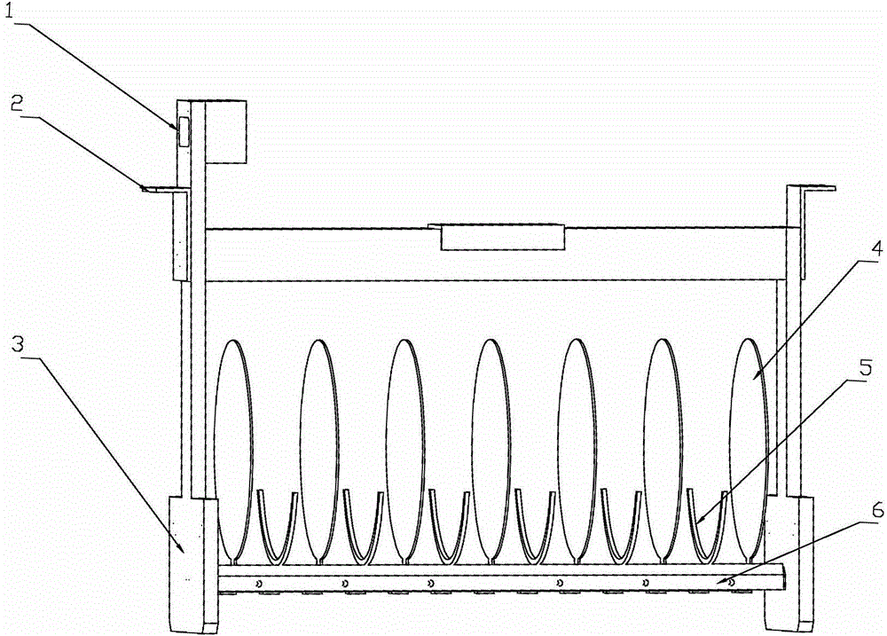
The invention relates to the technical field of passivation protection of chips of semiconductor devices, in particular to a table chip double side electrophoresis glass passivation technology. The table chip double side electrophoresis glass passivation technology includes: using a modified electrophoresis frame, directly placing a silicon slice in an anodic metal half ring so as to use the silicon slice as an anodic plate, and placing negative plates on two sides of the anodic plate for electrophoresis. Accordingly, distances from table grooves in two sides of the silicon slice to the negative plates are equal, electric field distribution is even, and glass layers of the same thickness can be formed. Furthermore, an appropriate electrophoresis solution proportion and a glass sintering technology in a wet oxygen atmosphere are used, and therefore consistency of a double face glass passivation layer can be improved, glass is in complete and uniform in modeling, and simultaneously qualified rate and reliability of products can be improved, surge resisting ability of the semiconductor devices is enhanced, and production efficiency can be improved.

Description

technical field [0001] The invention relates to the technical field of chip passivation protection for semiconductor devices, in particular to a double-sided electrophoretic glass passivation process for mesa chips. Background technique [0002] At present, mesa chips of some devices in the semiconductor industry, such as discharge tubes, bidirectional TVS diodes, and triacs, generally require double-sided passivation protection. Commonly used glass passivation protection processes include knife scraping, photoresisting, and electrophoresis. The knife scraping method has the disadvantages of uneven glass layer and poor reliability; the photoresist method has the problems of high cost and complicated process; the electrophoresis method has the advantages of simple process and high reliability and is applied to the passivation protection of the mesa chip. However, the commonly used double-sided electrophoresis method is usually the process of electrophoresis on one side and th...

Claims


Application Information

Patent Timeline
IPC IPC(8): H01L21/311
CPCH01L21/31111
Inventor 丛培金范玉丰丛济洲
Owner SUZHOU QILAN POWER ELECTRONICS
Learn More