Manufacturing method and product of high-conductivity and low-reflectivity metal mesh

A metal grid, low reflectivity technology, applied in electrical digital data processing, data processing input/output process, instruments, etc. Long exposure time and other problems, to achieve the effect of reducing reflectivity, easy operation, and simple preparation process

Active Publication Date: 2015-05-13
福建省诺希科技园发展有限公司
View PDF4 Cites 7 Cited by
  • Summary
  • Abstract
  • Description
  • Claims
  • Application Information

AI Technical Summary

Problems solved by technology

Although the above-mentioned production process can obtain a silver metal grid with a line width of less than 40 microns, as the size of the touch panel required by the market becomes larger and larger, the dimensional accuracy of the exposure machine of the yellow light process will become more and more accurate. Difficult to control, the width of the silver metal grid line is often different, and in the process of cleaning and removing other ions except silver particles, the problem of silver line breakage often occurs; the larger the size of the touch panel, the The longer the overall exposure time, the higher the cost
In addition, the above production process is only suitable for the preparation of silver metal grids, not suitable for metal grids of other low-resistance metal materials, such as copper metal grids, gold metal grids, etc.

Method used


Image

  • Manufacturing method and product of high-conductivity and low-reflectivity metal mesh
  • Manufacturing method and product of high-conductivity and low-reflectivity metal mesh
  • Manufacturing method and product of high-conductivity and low-reflectivity metal mesh

Examples


Embodiment approach

[0028] A method for manufacturing a metal grid with high conductivity and low reflectivity, comprising the following steps:

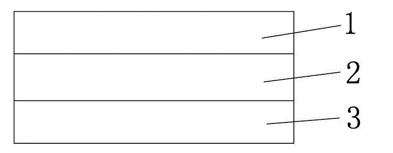
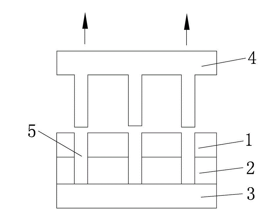
[0029] (1) Coating photoresist layers (1, 2) on the transparent substrate 3, the thickness of the photoresist layer is 20-60 microns, and the photoresist layer is formed by stacking two layers of photoresist layers with different etching rates (such as Figure 1~3 shown); and, the plasma etching rate of the photoresist material selected for the upper photoresist layer 1 is greater than the plasma etching rate of the photoresist material selected for the lower photoresist layer 2;

[0030] (2) The photoresist layer (1, 2) is imprinted by using the embossing template 4 with a raised circuit pattern on the bottom, and after the embossing template 4 is pulled out, a circuit pattern is formed in the photoresist layer (1, 2) Groove 5 (eg figure 2 shown);

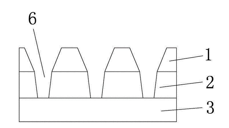
[0031] (3) Carry out plasma etching to the photoresist layer (1, 2) after embossing, expose transpare...


PUM

PropertyMeasurementUnit
thicknessaaaaaaaaaa

Abstract

The invention provides a manufacturing method of a high-conductivity and low-reflectivity metal mesh. The processing technologies of photoresist layer coating, embossing, plasma etching, metal mesh material plating and cleaning are adopted. The thickness of a photoresist layer is 20-60 microns, the photoresist layer is formed by two photoresist layer bodies with different etching rates in an overlaying mode, and the plasma etching rate of a photoresist material selected by the upper photoresist layer body is larger than the plasma etching rate of a photoresist material selected by the lower photoresist layer body. The plasma etching condition is that plasma power is 2000-3000 W, and the etching time is 2-30 minutes. The manufacturing method can be used for manufacturing the metal mesh with the width of an outgoing line being lower than 40 microns, and is suitable for manufacturing metal meshes which are made of all low resistance value metal materials such as gold, silver, copper and aluminium. In addition, the metal mesh which is manufactured by the method and is provided with a wide upper portion and a narrow lower portion has the advantages of being low in reflectivity and high in conductivity.

Description

technical field [0001] The invention belongs to the field of touch panel materials, in particular to a method for manufacturing a high-conductivity and low-reflectivity metal grid and a product thereof. Background technique [0002] In the future, mobile terminals, wearable devices, smart home appliances and other products will have a strong demand for touch panels. At the same time, with the large size and low price of touch panels, and the traditional ITO film can not be used for flexible applications, the conductivity and light transmission Due to factors such as the difficulty of overcoming essential problems such as high efficiency, many panel manufacturers have begun to study alternatives to ITO, including materials such as nano-silver wires, metal grids, carbon nanotubes, and graphene. Among them, the metal grid is most widely used in the market because of its lowest cost and good electrical conductivity. [0003] The traditional production process of metal mesh (Met...

Claims


Application Information

Patent Timeline
Patent Type & Authority Applications(China)
IPC IPC(8): G06F3/041
CPCG06F3/0412G06F2203/04103
Inventor 林杰侯则良王维纲
Owner 福建省诺希科技园发展有限公司
Why Eureka
Try Eureka