Diamond schottky diode and manufacturing method thereof

A technology of Schottky diode and manufacturing method, which is applied in semiconductor/solid-state device manufacturing, electrical components, circuits, etc., can solve the problem that the current density cannot meet the Achilles heel of power devices, and achieves the goal of reducing leakage current and improving reverse performance. Effect

Inactive Publication Date: 2015-05-13
王宏兴
View PDF5 Cites 6 Cited by
  • Summary
  • Abstract
  • Description
  • Claims
  • Application Information

AI Technical Summary

Problems solved by technology

In recent years, with the extensive development of aerospace, electric locomotives, electric vehicles, and DC high-voltage transmission, semiconductor power conversion devices have put forward requirements for high withstand voltage, high current, high efficiency, low loss, and high temperature resistance. Due to their inherent characteristics, the existing semiconductor materials have gradually revealed the Achilles heel that cannot meet the requirements of power devices in terms of breakdown field strength, self-heating effect, and current density.

Method used


Image

  • Diamond schottky diode and manufacturing method thereof
  • Diamond schottky diode and manufacturing method thereof
  • Diamond schottky diode and manufacturing method thereof

Examples


Embodiment Construction

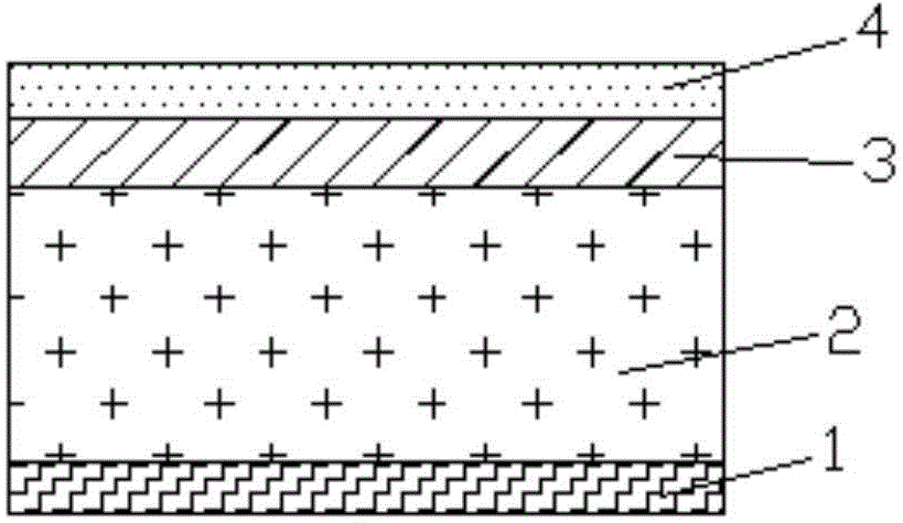
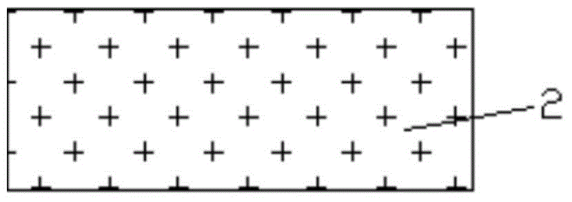
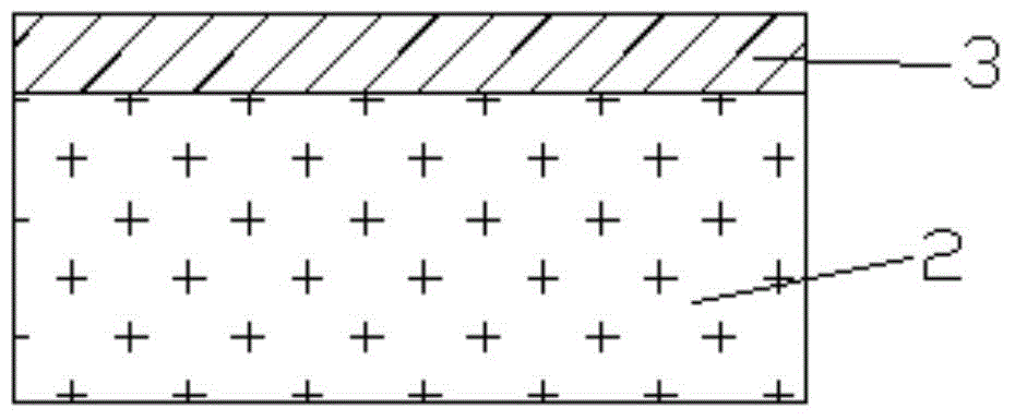
[0020] The main structure of the diamond Schottky diode is a metal electrode and a P-type (boron-doped) diamond film to form a diode. One of its important applications is high-voltage, high-current, and high-temperature high-power power conversion. At present, the P-type doping of diamond is relatively mature. The diamond Schottky diode made of P-type doped diamond has the advantages of low turn-on voltage, good high temperature resistance, large rectification ratio and fast switching speed. Since the breakdown electric field of diamond is much larger than that of other semiconductors, under the same withstand voltage requirements, diamond Schottky diodes can be made thinner and have smaller on-resistance. And because of its high thermal conductivity, it can effectively dissipate heat and have better stability.

[0021] In order to optimize the performance of diamond Schottky diodes, scientists have been trying to use different metals as the Schottky electrodes of diamond Scho...


PUM


Abstract

The invention discloses a diamond schottky diode and a manufacturing method thereof. The diamond schottky diode comprises an ohmic electrode, a P-type highly-doped diamond substrate, a drift layer and a schottky electrode which are laminated in sequence, wherein the schottky electrode is of a single hafnium layer structure or a composite layer structure comprising a plurality of single metal layers with a single hafnium layer as a bottom layer. According to the diamond schottky diode manufactured by the method, the withstand voltage is improved, the reverse leakage current is reduced, and the reverse performance of the diamond schottky diode is improved.

Description

technical field [0001] The invention belongs to the technical field of semiconductor devices, and in particular relates to a diamond Schottky diode and a manufacturing method thereof. Background technique [0002] Diamond is composed of carbon atoms and belongs to the cubic crystal system, and its structure is a compound lattice in which the Bravais lattice is a face-centered cubic. Its high band gap (5.5eV), high breakdown field strength (10MV / cm), high electron and hole mobility (4500cm 2 / (V·s) and 3800cm 2 / (V·s)) and high thermal conductivity (22W / (mm·K)), making diamond have great potential in high-frequency, high-efficiency, high-power, high-temperature fields such as power energy electronics, information electronics, environmental electronics, etc. Wide application prospects. And with the development of microwave plasma chemical vapor deposition (MPCVD) technology, more and more semiconductor devices are made of diamond, and their performance is getting better and...

Claims


Application Information

Patent Timeline
IPC IPC(8): H01L29/872H01L29/16H01L21/329
Inventor 王宏兴胡超王玮张景文卜忍安侯洵
Owner 王宏兴
Why Eureka
Try Eureka