CIGS (Copper Indium Gallium Selenide)-based thin film solar cell and preparation method thereof

A thin-film solar cell, prefabricated layer technology, applied in circuits, photovoltaic power generation, electrical components, etc., can solve the problems of low cell conversion efficiency and unsatisfactory light absorption layer crystallization, and achieve the effect of high photoelectric conversion efficiency

Active Publication Date: 2015-05-13
厦门神科太阳能有限公司
View PDF3 Cites 6 Cited by
  • Summary
  • Abstract
  • Description
  • Claims
  • Application Information

AI Technical Summary

Problems solved by technology

[0006] The main purpose of the present invention is to solve the problems in the prior art: during the selenization and/or vulcanization process, the sodium ions in the glass substrate will

Method used


Image

  • CIGS (Copper Indium Gallium Selenide)-based thin film solar cell and preparation method thereof
  • CIGS (Copper Indium Gallium Selenide)-based thin film solar cell and preparation method thereof
  • CIGS (Copper Indium Gallium Selenide)-based thin film solar cell and preparation method thereof

Examples


Embodiment 1

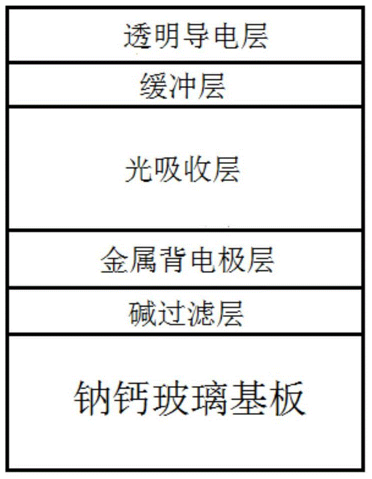
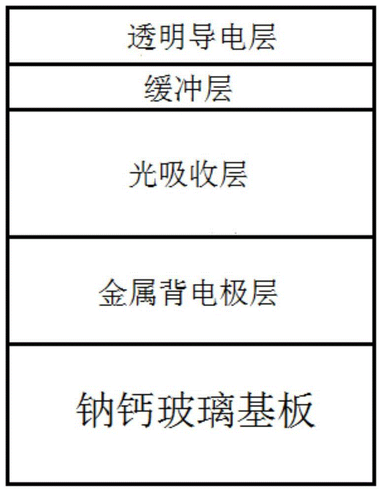
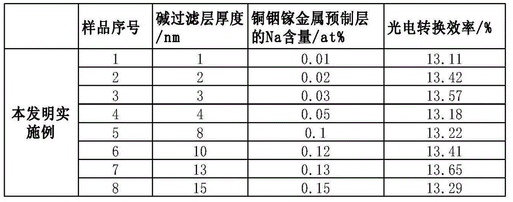
[0026] One deck of LiOa-AlOb-SiOc alkali filter layer (a=0.5, b=1.5, c=2) containing 0.005wt% Li is sputter deposited on the soda-lime glass substrate surface, and in the alkali filter layer, Si:Al=9: 1 (mass ratio), then sputter-deposit a 500nm molybdenum back electrode layer on the alkali filter layer, then deposit a copper indium gallium metal prefabricated layer containing Na on the molybdenum back electrode layer, and then send the sample into a heating furnace for selenization Heat treatment to form a light-absorbing layer, then deposit a 40nm cadmium sulfide film in a water bath on the light-absorbing layer, then deposit a 50nm ZnO film on the cadmium sulfide layer, and then deposit a 600nm AZO transparent conductive film on the ZnO film. The results of Example 1 of the present invention are shown in Table 1 below.

[0027] Table 1

[0028]

Embodiment 2

[0030]LiOa-AlOb-SiOc alkali filter layer (a=0.45, b=1.4, c=1.9) containing 5wt% Li is deposited on the surface of soda-lime glass substrate by sputtering, and Si:Al=9:1 in the alkali filter layer (mass ratio), then sputter-deposit a 500nm molybdenum back electrode layer on the alkali filter layer, then deposit a copper indium gallium metal prefabricated layer containing Na on the molybdenum back electrode layer, and then send the sample into a heating furnace for selenization heat treatment , forming a light absorbing layer, then depositing a 40nm cadmium sulfide film layer in a water bath on the light absorbing layer, then depositing a 50nm ZnO film layer on the cadmium sulfide layer, and then depositing a 600nm AZO transparent conductive film layer on the ZnO film layer. The results of Example 2 of the present invention are shown in Table 2 below.

[0031] Table 2

[0032]

Embodiment 3

[0034] LiOa-AlOb-SiOc alkali filter layer (a=0.5, b=1.5, c=2) containing 1wt% Li is sputter deposited on the surface of soda-lime glass substrate, and Si:Al=9:1 in the alkali filter layer (mass ratio), then sputter-deposit a 500nm molybdenum back electrode layer on the alkali filter layer, then deposit a copper indium gallium metal prefabricated layer containing Na on the molybdenum back electrode layer, and then send the sample into a heating furnace for selenization heat treatment , forming a light absorbing layer, then depositing a 40nm cadmium sulfide film layer in a water bath on the light absorbing layer, then depositing a 50nm ZnO film layer on the cadmium sulfide layer, and then depositing a 600nm AZO transparent conductive film layer on the ZnO film layer. The results of Example 3 of the present invention are shown in Table 3 below.

[0035] table 3

[0036]


PUM

PropertyMeasurementUnit
Thicknessaaaaaaaaaa
Thicknessaaaaaaaaaa

Abstract

The invention discloses a CIGS (Copper Indium Gallium Selenide)-based thin film solar cell and a preparation method thereof. The preparation method comprises the following steps: forming an alkali filter layer containing at least one element of Li and K on a glass substrate; forming a back electrode layer on the alkali filter layer; forming a light absorption layer on the back electrode; forming a buffer layer on the light absorption layer; forming an n-type transparent conductive layer on the buffer layer, and is characterized by being provided with the alkali filter layer with certain thickness to allow a part of alkali metal ions to be diffused into the CIGS-based light absorption layer from the glass substrate, wherein a certain amount of alkali metal is further added on the outer side of the CIGS-based light absorption layer.

Description

technical field [0001] The invention relates to the technical field of thin film solar cells, in particular to an alkali filter layer of a copper indium gallium selenide (sulfur) thin film cell with a chalcopyrite structure and a preparation method thereof. Background technique [0002] With the global warming, the deterioration of the ecological environment and the shortage of conventional energy, more and more countries have begun to vigorously develop solar energy utilization technology. Solar photovoltaic power generation is a zero-emission clean energy, which has the advantages of safety, reliability, no noise, no pollution, inexhaustible resources, short construction period, and long service life, so it has attracted much attention. Copper indium gallium selenide (CIGS) is a direct bandgap P-type semiconductor material with an absorption coefficient as high as 10 5 / cm, 2um thick copper indium gallium selenide film can absorb more than 90% of sunlight. The band gap o...

Claims


Application Information

Patent Timeline
IPC IPC(8): H01L31/18H01L31/0392H01L31/0749
CPCH01L31/0392H01L31/0749H01L31/18Y02E10/541Y02P70/50
Inventor 李艺明田宏波
Owner 厦门神科太阳能有限公司
Why Eureka
Try Eureka