ldmos device and manufacturing method
A device and manufacturing process technology, applied in the field of LDMOS device manufacturing, can solve problems such as low on-resistance, reduce device breakdown voltage, etc., achieve large on-resistance, increase breakdown voltage, and reduce on-resistance
- Summary
- Abstract
- Description
- Claims
- Application Information
AI Technical Summary
Problems solved by technology
Method used
Image
Examples
Embodiment Construction
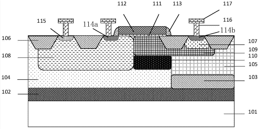
[0048] figure 1 It is a schematic structural diagram of an LDMOS device in an embodiment of the present invention; the LDMOS device in an embodiment of the present invention is an N-type LDMOS device, including:
[0049] The N+ buried layer 102 is formed on the P-type silicon substrate 101 .
[0050] The P+ buried layer 103 is formed on a part of the N+ buried layer 102 , and the bottom of the P+ buried layer 103 is in contact with the N+ buried layer 102 .
[0051] The N-type epitaxial layer 104 is formed on the surface of the silicon substrate 101 , and the bottom of the N-type epitaxial layer 104 is respectively in contact with the N+ buried layer 102 and the P+ buried layer 103 .
[0052] The P-type diffusion layer 105 is formed in the N-type epitaxial layer 104 on the top of the P+ buried layer 103, and the P-type impurities of the P-type diffused layer 105 are transferred from the P+ buried layer 103 to the N-type epitaxial layer. Diffusion formation in 104.
[0053] ...
PUM
 Abstract
Description
Claims
Application Information


