Nitrogen dioxide gas sensor and preparation and testing methods of nitrogen dioxide gas sensor

A gas sensor and nitrogen dioxide technology, applied in the sensor field, can solve the problems of deteriorating the properties of organic semiconductor polymers, etc., and achieve the effects of favorable electrical performance, low production cost, and improved mobility

Inactive Publication Date: 2015-06-03
UNIV OF ELECTRONICS SCI & TECH OF CHINA
View PDF3 Cites 11 Cited by
  • Summary
  • Abstract
  • Description
  • Claims
  • Application Information

AI Technical Summary

Problems solved by technology

However, most of the current reports indicate that the doping of semiconductor oxides in organic semiconductors will deteriorate the performance of organic semiconductor polymers.

Method used


Image

  • Nitrogen dioxide gas sensor and preparation and testing methods of nitrogen dioxide gas sensor
  • Nitrogen dioxide gas sensor and preparation and testing methods of nitrogen dioxide gas sensor
  • Nitrogen dioxide gas sensor and preparation and testing methods of nitrogen dioxide gas sensor

Examples


Embodiment 1

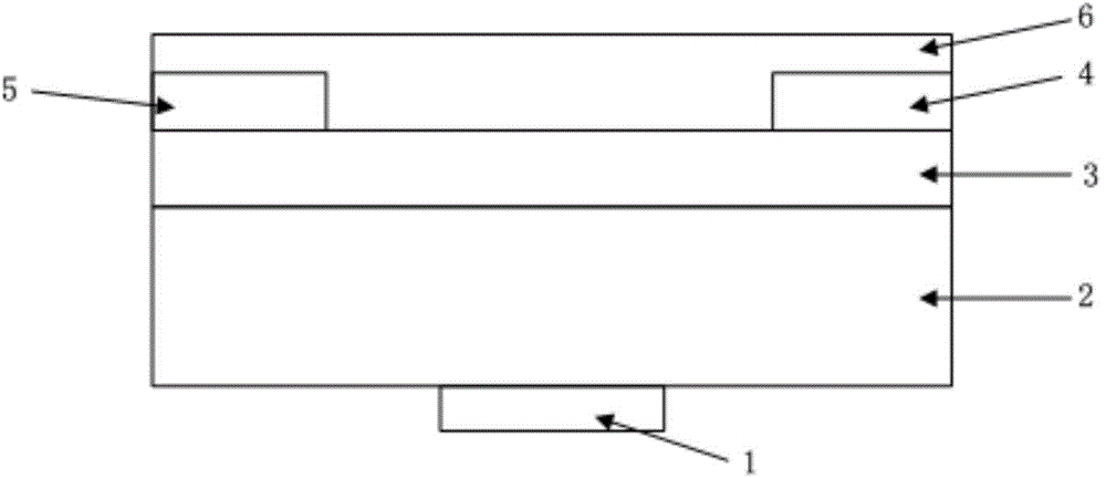
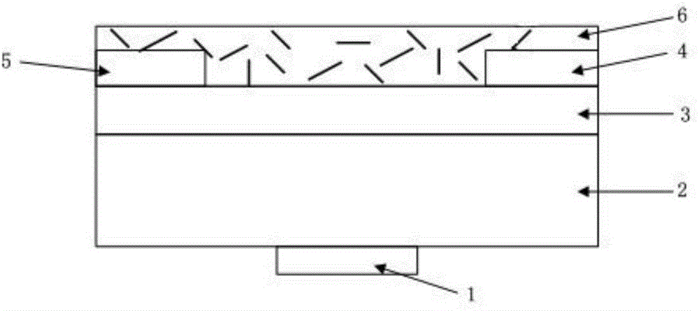
[0036] A nitrogen dioxide gas sensor, the structure of which is an organic thin film field effect transistor, comprising a gate electrode 1, a substrate 2 above the gate electrode 1, an oxide gate layer 3 above the substrate 2, and a source electrode 4 above the oxide gate layer 3 And the drain electrode 5, the active layer 6 above the source electrode 4 and the drain electrode 5, wherein the substrate is a silicon substrate, the oxide gate layer 3 is silicon dioxide, the source electrode, the gate electrode and the drain electrode are gold electrodes, and the active layer It is a composite film formed by combining ZnO nanorods and P3HT polymer. The diameter of the ZnO nanorods is 100 nm, and the length of the ZnO nanorods is 0.5 μm. In the active layer, the mass ratio of P3HT polymer and ZnO nanorods is 6:1. The sensor is a field effect transistor gas sensor with bottom gate and bottom contact. The thickness of the active layer thin film is 60nm-90nm.

[0037] The preparat...

Embodiment 2

[0043] A nitrogen dioxide gas sensor, the structure of which is an organic thin film field effect transistor, comprising a gate electrode 1, a substrate 2 above the gate electrode 1, an oxide gate layer 3 above the substrate 2, and a source electrode 4 above the oxide gate layer 3 And the drain electrode 5, the active layer 6 above the source electrode 4 and the drain electrode 5, wherein the substrate is a silicon substrate, the oxide gate layer 3 is silicon dioxide, the source electrode, the gate electrode and the drain electrode are gold electrodes, and the active layer It is a composite film formed by combining ZnO nanorods and P3HT polymer.

[0044] The diameter of the ZnO nanorods is 250 nm, and the length of the ZnO nanorods is 4 μm. In the active layer, the mass ratio of P3HT polymer and ZnO nanorods is 6:2. The sensor is a field effect transistor gas sensor with bottom gate and bottom contact.

[0045] The thickness of the active layer thin film is 60nm-90nm.

[00...

Embodiment 3

[0052] A nitrogen dioxide gas sensor, its structure is an organic thin film field effect transistor, including a gate electrode 1, a substrate 2, an oxide gate layer 3, a source electrode 4 and a drain electrode 5, and an active layer 6, wherein the substrate is a silicon lining The bottom, the oxide gate layer 3 is silicon dioxide, the source electrode, gate electrode and drain electrode are gold electrodes, and the active layer is a composite material film formed by compounding ZnO nanorods and P3HT polymer.

[0053] The diameter of the ZnO nanorods is 150 nm, and the length of the ZnO nanorods is 2 μm.

[0054] In the active layer, the mass ratio of P3HT polymer and ZnO nanorods is 6:6.

[0055] The sensor is a field effect transistor gas sensor with bottom gate and bottom contact.

[0056] The thickness of the active layer thin film is 60nm-90nm.

[0057] The preparation method of the above-mentioned nitrogen dioxide gas sensor comprises the following steps:

[0058] ①D...


PUM

PropertyMeasurementUnit
diameteraaaaaaaaaa
lengthaaaaaaaaaa
thicknessaaaaaaaaaa

Abstract

The invention provides a nitrogen dioxide gas sensor and preparation and testing methods of the nitrogen dioxide gas sensor. The sensor structure is an organic thin-film field effect transistor, and comprises a gate electrode, a substrate, a gate oxide layer, a source electrode and a drain electrode, as well as an active layer; the active layer is a composite thin film formed by compounding ZnO nanorods and a P3HT polymer; the preparation method comprises the following steps: (1) preparing the ZnO nanorods by use of a low-temperature hydrothermal method; (2) depositing a P3HT-ZnO composite material on the source electrode and the drain electrode by use of a spraying film-forming method, wherein the ZnO nanorods are in contact with the P3HT polymer to form a heterojunction structure; the sensor is capable of effectively increasing the migration rate of the OTFT device and the response of the gas sensor to a gas to be tested; the film forming process is simple, the production cost is low, the electrical properties of the FET device can be improved favorably, and the response of the gas sensor can be effectively improved according to the change of the potential barrier of the interface after the molecules of the gas to be tested are adsorbed on the interface of the formed heterojunction structure.

Description

technical field [0001] The invention relates to the technical field of sensors, in particular to a nitrogen dioxide gas sensor working at room temperature, a preparation method and a testing method thereof. Background technique [0002] Since humans entered the information society at the end of the 20th century, all human activities have centered on information acquisition and information exchange. As the foundation of information technology and one of the three pillars, sensor technology has also entered a new era of rapid development. [0003] Since the sensitive layer of the OTFT gas sensor is also the active layer of the FET device, the performance of the sensitive layer film is very important. The selection of the sensitive layer should not only meet the special requirements of FET transistors, such as high carrier mobility and low intrinsic conductance, but also be sensitive to the gas to be measured. This puts forward very high requirements for sensitive materials, a...

Claims


Application Information

Patent Timeline
Patent Type & Authority Applications(China)
IPC IPC(8): G01N27/414
Inventor 谢光忠解涛杜鸿飞黄俊龙杜晓松太惠玲蒋亚东
Owner UNIV OF ELECTRONICS SCI & TECH OF CHINA
Why Eureka
Try Eureka