4H-SiC metal-semiconductor field effect transistor with double-sunken buffer layer

A field-effect transistor and metal-semiconductor technology, which is applied in the field of 4H-SiC metal-semiconductor field-effect transistors, can solve the problems that the saturation leakage current has not been substantially improved, the drain current is reduced, and the saturation current is degraded, so as to avoid the breakdown voltage Effects of sharp drop, increase in saturation leakage current, and increase in drain current

Active Publication Date: 2015-06-03
XIDIAN UNIV
View PDF2 Cites 10 Cited by
  • Summary
  • Abstract
  • Description
  • Claims
  • Application Information

AI Technical Summary

Problems solved by technology

[0004] Although the breakdown voltage of the double-recess structure 4H-SiC MESFET is increased due to the fact that half the length of the source side of the gate is recessed into the N-type channel layer, the saturation leakage current has not been substantially improved.
And in practice, the process of reactive ion etching (RIE) will form lattice damage on the surface of the drift region of the device, resulting in a decrease in the effective mobility of carriers in the N-type channel layer, thereby reducing the drain current. In terms of current output characteristics manifested as a degradation of the saturation current

Method used


Image

  • 4H-SiC metal-semiconductor field effect transistor with double-sunken buffer layer
  • 4H-SiC metal-semiconductor field effect transistor with double-sunken buffer layer

Examples


Embodiment 1

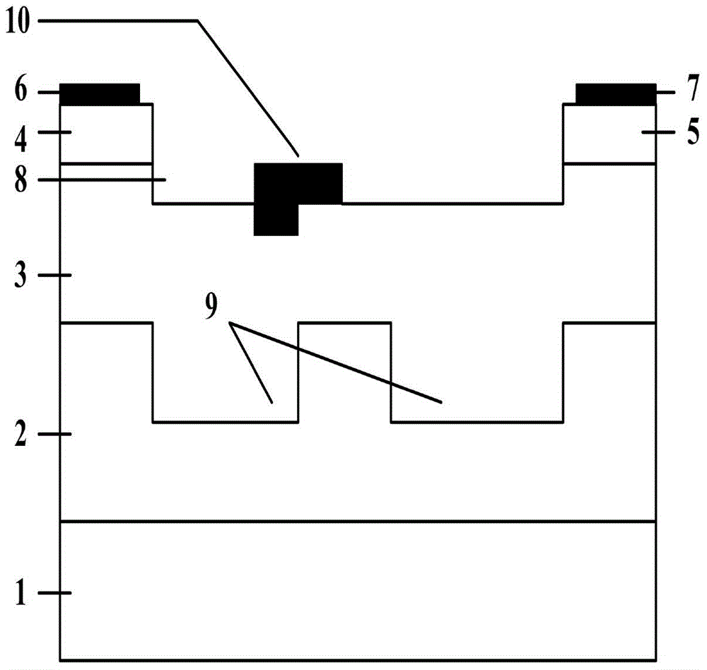
[0028] The production thickness is A 4H-SiC metal-semiconductor field-effect transistor with a thickness of 0.25 μm, starting from the inner side of the source cap layer and the drain cap layer, and a double-recessed buffer layer with a length of 0.85 μm and 0.8 μm respectively.

[0029] The manufacturing steps of this embodiment are as follows:

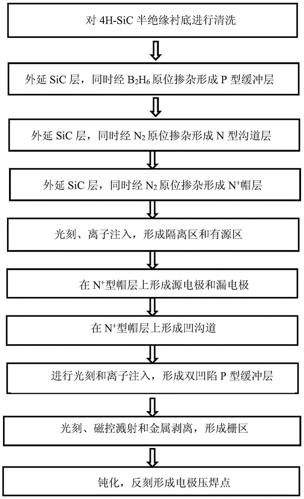
[0030] Step 1: cleaning the 4H-SiC semi-insulating substrate 1 to remove surface pollutants.

[0031] (1) The substrate was carefully cleaned twice with a cotton ball dipped in methanol to remove SiC particles of various sizes on the surface;

[0032] (2) Place 4H-SiC semi-insulating substrate 1 in H 2 SO 4 :HNO 3 = Ultrasound for 5 minutes in 1:1;

[0033] (3) Put the 4H-SiC semi-insulating substrate 1 in 1# cleaning solution (NaOH:H 2 o 2 :H 2 O=1:2:5), boiled for 5 minutes, rinsed with deionized water for 5 minutes, and then put into 2# cleaning solution (HCl:H 2 o 2 :H 2 O=1:2:7) and boiled for 5 minutes. Finally rin...

Embodiment 2

[0070] The production thickness is And a 4H-SiC metal semiconductor field effect transistor with a thickness of 0.2 μm, starting from the inner side of the source cap layer and the drain cap layer, and a double recessed buffer layer with a length of 0.85 μm and 0.8 μm respectively. In the manufacturing steps of this embodiment:

[0071] Step 8: performing a photolithography and ion implantation to form a double recessed P-type buffer layer 9 .

[0072] (1) Positive photoresist is used, glue coating speed: 3000R / min, glue thickness Ensure that it can play a good blocking role in the subsequent isolation injection;

[0073] (2) After gluing is completed, pre-bake in an oven at 90°C for 90 seconds, and use a double-depressed buffer layer photolithography plate for about 35 seconds of UV exposure in a special developer solution (tetramethylammonium hydroxide: water = 1:3) Develop for 60 seconds, then post-bake in an oven at 100°C for 3 minutes;

[0074] (3) Perform nitrogen ...

Embodiment 3

[0078] The production thickness is And a 4H-SiC metal semiconductor field effect transistor with a thickness of 0.3 μm, starting from the inner side of the source cap layer and the drain cap layer, and a double recessed buffer layer with a length of 0.85 μm and 0.8 μm respectively. In the manufacturing steps of this embodiment:

[0079] Step 8: performing a photolithography and ion implantation to form a double recessed P-type buffer layer 9 .

[0080] (1) Positive photoresist is used, glue coating speed: 3000R / min, glue thickness Ensure that it can play a good blocking role in the subsequent isolation injection;

[0081] (2) After gluing is completed, pre-bake in an oven at 90°C for 90 seconds, and use a double-depressed buffer layer photolithography plate for about 35 seconds of UV exposure in a special developer solution (tetramethylammonium hydroxide: water = 1:3) Develop for 60 seconds, then post-bake in an oven at 100°C for 3 minutes;

[0082] (3) Perform nitrogen ...


PUM


Abstract

The invention discloses a 4H-SiC metal-semiconductor field effect transistor with a double-sunken buffer layer. The 4H-SiC metal-semiconductor field effect transistor comprises a 4H-SiC semi-insulating substrate, a P type buffer layer and an N type channel layer from bottom to top, wherein a source electrode cap layer and a drain electrode cap layer are respectively arranged on two sides of the N type channel layer; a source electrode and a drain electrode are respectively arranged on the surfaces of the source electrode cap layer and the drain electrode cap layer; a gate electrode is formed on one side, close to the source electrode cap layer, above a channel; grooves are arranged on the upper end face of the P type buffer layer and under a gate source and a gate leakage. The 4H-SiC metal-semiconductor field effect transistor has the advantages that the output drain electrode current is obviously improved, and the breakdown voltage is stable.

Description

technical field [0001] The invention relates to the technical field of field effect transistors, in particular to a 4H-SiC metal semiconductor field effect transistor with double recessed buffer layers. Background technique [0002] SiC materials have outstanding material and electrical properties such as wide band gap, high breakdown electric field, high saturation electron migration velocity, and high thermal conductivity, making them suitable for high-frequency and high-power device applications, especially high temperature, high voltage, aerospace, satellite, etc. It has great potential in high-frequency high-power device applications in harsh environments. In SiC allomorphs, the electron mobility of 4H-SiC with hexagonal close-packed wurtzite structure is nearly three times that of 6H-SiC, so 4H-SiC materials are used in high-frequency and high-power devices, especially in metal-semiconductor fields. Effect transistor (MESFET) occupies a major position in the applicati...

Claims


Application Information

Patent Timeline
Patent Type & Authority Applications(China)
IPC IPC(8): H01L29/78H01L29/10
Inventor 贾护军张航邢鼎
Owner XIDIAN UNIV
Why Eureka
Try Eureka