

Intermetallic compound bonding method and structure for three-dimensionally packaged chip stacking
An intermetallic compound and chip stacking technology, which is applied in metal processing equipment, electrical components, circuits, etc., can solve the problems of low bonding strength, long bonding time, and low efficiency, and improve mechanical properties and service life. Reliability, improved bonding efficiency, and good process compatibility
- Summary
- Abstract
- Description
- Claims
- Application Information
AI Technical Summary
Problems solved by technology
Method used
Image

Examples
Embodiment 1
[0055] The intermetallic compound bonding method for three-dimensional packaging chip stacking of the present invention is realized through the following specific process steps:
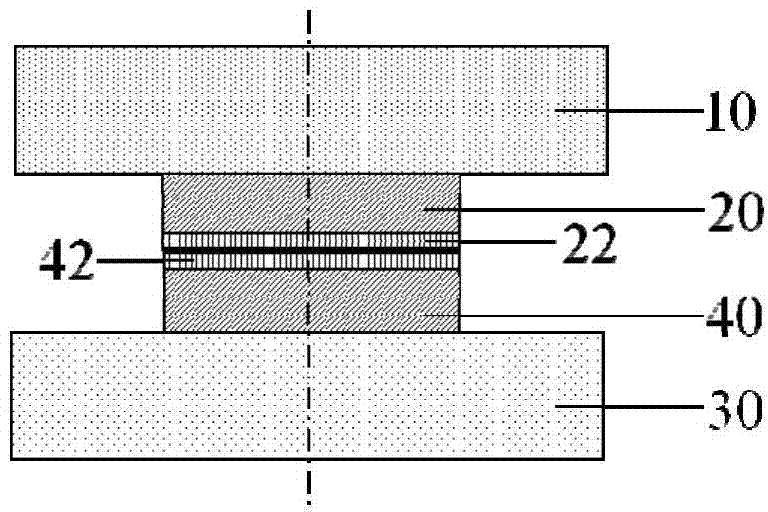
[0056] Step 1: Provide a chip first substrate 10, electroplate a 5 μm thick array of Cu first metal bumps 20 on the chip first substrate 10, and electroplate a 5 μm thick Sn The first solder layer 22; provide the second substrate 30 of the chip, on the second substrate 30 of the chip, electroplate an array of Cu second metal bumps 40 with a thickness of 15 μm, and electroplate on the second Cu metal bumps 40 5 μm thick Sn second solder layer 42; Cu first metal bumps 20 and Cu second metal bumps 40 have a mirror-symmetrical array pattern;
[0057] Step 2: align the first Sn solder layer 22 and the second Sn solder layer 42 one by one, and place them in face-to-face contact to form an assembly, such as figure 1 shown;
[0058] Step 3: Heating the assembly formed in Step 2 and performing brazing reflo...
Embodiment 2
[0061] The intermetallic compound bonding method for three-dimensional packaging chip stacking of the present invention is realized through the following specific process steps:
[0062] Step 1: Provide a chip first substrate 10, electroplate a 5 μm thick array of Cu first metal bumps 20 on the chip first substrate 10, and electroplate a 10 μm thick Sn The first solder layer 22; the second substrate 30 of the wafer is provided, and an array of Cu second metal bumps 40 with a thickness of 25 μm is electroplated on the second substrate 30 of the wafer, and the second metal bumps 40 of Cu are electroplated. Electroplating a 10 μm thick Sn second solder layer 42; Cu first metal bumps 20 and Cu second metal bumps 40 have a mirror-symmetrical array pattern;
[0063] Step 2: align the first Sn solder layer 22 and the second Sn solder layer 42 one by one, and place them in face-to-face contact to form an assembly, such as figure 1 shown;
[0064] Step 3: Heating the assembly formed ...
Embodiment 3
[0067] The intermetallic compound bonding method for three-dimensional packaging chip stacking of the present invention is realized through the following specific process steps:
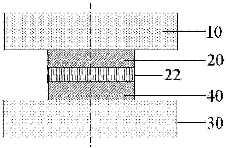
[0068] Step 1: Provide a wafer first substrate 10, electroplate an array of Cu first metal bumps 20 with a thickness of 5 μm on the first wafer substrate 10, and electroplate an array of Cu first metal bumps 20 with a thickness of 30 μm A first solder layer 22 of Sn; a second wafer substrate 30 is provided, on which a 30 μm thick array of Cu second metal bumps 40 is electroplated; Cu first metal bumps 20 and Cu second metal bumps 40 have a mirror-symmetrical array pattern;
[0069] Step 2: Align the Sn first solder layer 22 with the Cu second metal bump 40 one by one, and place them in face-to-face contact to form an assembly, such as figure 2 shown;
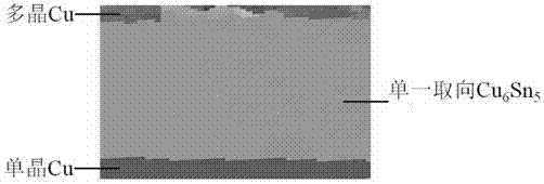
[0070] Step 3: Heating the assembly formed in Step 2 and performing brazing reflow, so that the temperature of the Cu first metal bump 20 reaches 2...
PUM
| Property | Measurement | Unit |
|---|---|---|
| thickness | aaaaa | aaaaa |
| thickness | aaaaa | aaaaa |
Abstract
Description
Claims
Application Information