TSV wafer surface polishing method

A surface polishing and wafer technology, applied in grinding devices, electrical components, grinding machine tools, etc., can solve the problems of high price of chemical mechanical polishing machines, inability to guarantee stable and uniform quality, long polishing time, etc. Surface quality, low cost, effect of improved quality

Active Publication Date: 2015-06-17
珠海天成先进半导体科技有限公司
View PDF5 Cites 7 Cited by
  • Summary
  • Abstract
  • Description
  • Claims
  • Application Information

AI Technical Summary

Problems solved by technology

That is, a polishing pad is attached to the circular rotating disk, and the vacuum disk is used to absorb the back of the wafer and press it on the polishing pad to give a certain pressure on the back of the wafer. Use the metal Cu polishing solution to infiltrate the polishing pad, and rotate the vacuum disk and the rotating disk at the same time. The purpose of removing the Cu layer is

Method used


Image

  • TSV wafer surface polishing method
  • TSV wafer surface polishing method
  • TSV wafer surface polishing method

Examples


Embodiment 1

[0033] This preferred embodiment is used to remove metal Cu and Ta on the surface of the TSV blind hole electroplating wafer. The thickness of the Cu layer is 15 μm, and the thickness of the Ta layer is 100 nm. After polishing, the depression at the blind hole on the wafer surface is less than 2 μm. Concrete implementation steps according to the present invention are as follows:

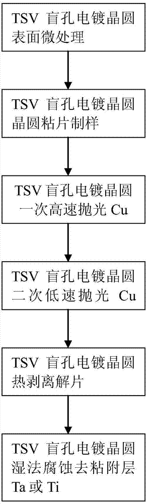
[0034] For the entire process, see figure 1 .

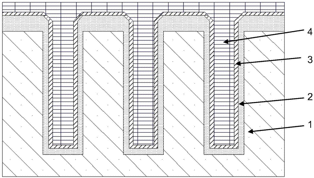
[0035] 1. First, surface treatment is performed on the surface of the TSV blind via plating wafer, see figure 2 , using H 2 SO 4 Solution and hydrogen peroxide mixed solution corrode thick Cu;

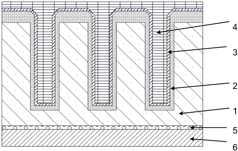
[0036] 2. Next, the wafer sample preparation process is carried out, and the wafer is bonded to the ceramic plate with a heat-peelable double-sided tape. See image 3 , and then the whole is placed on the rotating disc attached with the polishing pad;

[0037] 3. Put pressure on the ceramic disk, use metal Cu polishing liquid, adjust the speed of the cera...

Embodiment 2

[0048] This embodiment is used to remove metal Cu and Ti on the surface of the TSV blind hole electroplating wafer. The thickness of the Cu layer is 30 μm, and the thickness of the Ti layer is 100 nm. After polishing, the depression at the blind hole on the wafer surface is less than 2 μm. According to the specific implementation steps of the present invention such as Figure 1 to Figure 6 As shown, the steps are as follows.

[0049] Step 1.H 2 SO 4 Corrosion of Cu layer on the surface of TSV blind via electroplating wafer by solution and hydrogen peroxide mixed solution, H 2 SO 4 The solution is concentrated H with a mass fraction of 98% 2 SO 4 Add 3 times the volume of H 2 O diluted, H 2 SO 4 The volume ratio of solution: hydrogen peroxide = 1:2, and the corrosion time is 8 minutes.

[0050] Step 2. Use Nitto 3139# hot-peeling double-sided tape to bond the TSV blind hole electroplating wafer process to prepare samples, the pressure is 0.2Mpa, and the pressure holdin...

Embodiment 3

[0056] This embodiment is used to remove metal Cu and Ti on the surface of the TSV blind hole electroplating wafer. The thickness of the Cu layer is 5 μm, and the thickness of the Ti layer is 100 nm. After polishing, the depression at the blind hole on the wafer surface is less than 2 μm. According to the specific implementation steps of the present invention such as Figure 1 to Figure 6 As shown, the steps are as follows.

[0057] Step 1.H 2 SO 4 Corrosion of Cu layer on the surface of TSV blind via electroplating wafer by solution and hydrogen peroxide mixed solution, H 2 SO 4 The solution is concentrated H with a mass fraction of 98% 2 SO 4 Add 10 times the volume ratio of H 2 O diluted, H 2 SO 4 The volume ratio of solution: hydrogen peroxide = 1:5, and the corrosion time is 6 minutes.

[0058] Step 2. Use Nitto 3139# tape heat-peelable double-sided tape to prepare samples for TSV blind via electroplating wafer process bonding, the pressure is 0.1Mpa, and the pre...


PUM

PropertyMeasurementUnit
Thicknessaaaaaaaaaa
Thicknessaaaaaaaaaa

Abstract

The invention provides a TSV wafer surface polishing method. Firstly, a copper layer on the surface of a TSV blind hole electroplated wafer is corroded through a H2SO4 solution and a hydrogen peroxide mixed solution; then, the wafer adheres to a ceramic plate through thermal spalling double-faced adhesive tape for the wafer sample preparation process; the whole wafer is placed on a rotary plate attached to a polishing pad for polishing and copper layer removal; finally, after the ceramic plate is heated and taken off, Ta or Ti corrosive liquid is adopted, a Ta or Ti blocking layer corresponding to the surface of the TSV blind hole electroplated wafer is removed, and polishing of the surface of the TSV wafer is finished. By adding micro-processing of the surface of the TSV blind hole electroplated wafer, the state of the surface of the blind hole electroplated wafer is improved, polishing of the copper layer is facilitated, and polishing cost is reduced. Process operation is simple, cost is low, and the method is suitable for wafers and fragments of different sizes. By means of the thermal spalling double-faced adhesive tape, thickness uniformity in the wafer sample preparation process can be improved, and quality of the surface of the polished TSV blind hole electroplated wafer is improved.

Description

technical field [0001] The invention relates to a process method for semiconductor processing, in particular to a method for polishing the surface of a TSV wafer. Background technique [0002] In the Through Silicon Via technology (TSV; Through Silicon Via) process, after a through hole is formed on the wafer, metal Cu is generally plated in the through hole to form a vertical electrical interconnection. After the wafer is electroplated, there will be a certain thickness of Cu layer on the wafer surface. Controlled by the size of the through hole and the electroplating time, the thickness of the Cu layer on the wafer surface is ten to tens of microns. The Cu layer on the wafer surface needs to be removed in order to perform subsequent processes on the wafer surface, such as gluing, photolithography, and the like. The removal effect of the thicker Cu layer will directly affect the subsequent process quality of the wafer surface. [0003] At present, the Cu layer on the wafe...

Claims


Application Information

Patent Timeline
IPC IPC(8): H01L21/768B24B37/04
Inventor 吴道伟李克中张波郑晓琼
Owner 珠海天成先进半导体科技有限公司
Why Eureka
Try Eureka