Efficient ingot casting semi-melting technology capable of achieving low dislocation density

A low dislocation and density technology, applied in single crystal growth, polycrystalline material growth, crystal growth, etc., can solve the problems of inconsistent crystal orientation, uneven growth crystal interface, and low photoelectric conversion efficiency of large grains, and achieve stable lifting , Guarantee the effect of product quality

Inactive Publication Date: 2015-06-24
青岛隆盛晶硅科技有限公司
View PDF4 Cites 11 Cited by
  • Summary
  • Abstract
  • Description
  • Claims
  • Application Information

AI Technical Summary

Problems solved by technology

The disadvantages of this invention are: (1) A layer of monocrystalline silicon trim or the monocrystalline silicon seed crystal disclosed in the embodiment is evenly laid on the bottom of the crucible. Crystalline silicon rods, larger particle size
Both are easy to form large grains, and the photoelectric conversion efficiency of large grains is low, reaching up to 17.2%; (2) The opening distance at the bottom of the heat insulation cage described in claim 6 is greater than the opening distance in the previous step. According to the analysis and calculation, the speed of lifting the heat insulation cage in the comparison file is getting faster and faster. Under the influence of the changing speed, the horizontal melting interface cannot be well maintained, so the initial growth interface is not enough when growing crystals. Flat, resulting in inconsistent crystal orientation during crystallization

Method used


Image

  • Efficient ingot casting semi-melting technology capable of achieving low dislocation density

Examples


Embodiment 1

[0019] The ingot semi-melting process is carried out according to the following steps:

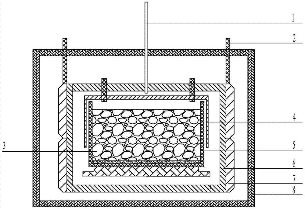
[0020] 1. Vacuumize the material and start heating: add the crushed single crystal with a particle size of 2mm to the bottom of the quartz crucible 5, the thickness of the pavement is 3cm, and then continue to add 450Kg of silicon material 3 into the quartz crucible 5, and control the furnace body 8 Evacuate to 0.5 Pa; control the heating of the heater 4 to evaporate the moisture of the graphite carbon felt 6 and the silicon material 3, etc., and raise the temperature to 1100 ° C within 2 hours, and pass the argon gas through the vent pipe 1 as a protective gas. Keep the pressure in the furnace body 8 at 40KPa, and make the temperature in the quartz crucible 5 reach 1545°C within 3 hours. During this process, the heat insulation cage 7 is always at 0 position (that is, closed state).

[0021] 2. Melting stage: Keep the pressure inside the furnace body 8 at 50KPa, keep the temperature of th...

Embodiment 2

[0026] The ingot semi-melting process is carried out according to the following steps:

[0027] 1. Vacuumize the material and start heating: add the crushed polycrystal with a particle size of 10mm to the bottom of the quartz crucible 5, the thickness of the pavement is 4cm, and then continue to add 500Kg of silicon material 3 into the quartz crucible 5, and control the furnace body 8 Vacuumize to 0.5 Pa; control the heating of the heater 4 to evaporate the moisture of the graphite carbon felt 6 and the silicon material 3, etc., and raise the temperature to 1200°C within 3 hours, and pass argon gas through the vent pipe 1 as a protective gas. Keep the pressure inside the furnace body 8 at 60KPa, and make the temperature inside the quartz crucible 5 reach 1560°C within 5 hours. During this process, the heat insulation cage 7 is always at 0 position (that is, closed state).

[0028] 2. Melting stage: Keep the pressure in the furnace body 8 at 50KPa, keep the temperature of the s...

Embodiment 3

[0033] The ingot semi-melting process is carried out according to the following steps:

[0034] 1. Vacuumize the material and start heating: add the crushed single crystal with a particle size of 15mm to the bottom of the quartz crucible 5, the thickness of the pavement is 4cm, and then continue to add 450Kg of silicon material 3 into the quartz crucible 5, and control the furnace body 8 Evacuate to 0.5Pa; control the heating of the heater 4 to evaporate the moisture of the graphite carbon felt 6 and the silicon material 3, etc., and raise the temperature to 1150°C within 2.5h, and pass argon gas through the vent pipe 1 as a protective gas , keep the pressure inside the furnace body 8 at 40KPa, make the temperature inside the quartz crucible 5 reach 1550°C within 4 hours, and during this process, the heat insulation cage 7 is always at 0 position (that is, closed state).

[0035] 2. Melting stage: Keep the pressure in the furnace body 8 at 50KPa, keep the temperature of the si...


PUM

PropertyMeasurementUnit
thicknessaaaaaaaaaa
particle diameteraaaaaaaaaa

Abstract

The invention belongs to the field of polycrystalline silicon ingot casting, and particularly relates to an efficient ingot casting semi-melting technology capable of achieving low dislocation density. The technology comprises loading vacuumizing, argon adding to achieve pressure rising, heating to achieve silicon mixture melting, crystal growing, annealing heat preservation and cooling. In the loading stage, firstly, a layer of broken single crystals or broken polycrystal is laid on the bottom inside a quartz crucible; in the melting stage, a heat insulation cage is improved at the speed of 0.5 cm / h to 1 cm / h, thus ensuring that the broken single crystals or broken polycrystal is not melted. The technological process can ensure that the silicon mixture can be sequentially and slowly melted from top to bottom, and a flat solid liquid interface is obtained; the temperature in the horizontal direction is coincident, the temperature gradient in the vertical direction is uniform, and some impurities and hard particles difficult to melt are ensured to be melted, and dislocation caused by the impurities and hard particles is reduced. The ingot casting dislocation density obtained through the technology is obviously reduced, the size of grains ranges from 6 mm to 8 mm, meanwhile, the photoelectric conversion efficiency of a solar cell piece is improved to 17.5 percent from 17.2 percent.

Description

technical field [0001] The invention belongs to the field of polysilicon ingot casting, and in particular relates to a high-efficiency ingot semi-melting process capable of realizing low dislocation density. Background technique [0002] Polycrystalline silicon is a form of elemental silicon. When molten elemental silicon solidifies under supercooled conditions, silicon atoms are arranged in the form of diamond lattices to form many crystal nuclei, and these nuclei grow into crystal grains with different crystal plane orientations. These crystal grains Joined together to form polysilicon. The process of producing solar photovoltaic products in the solar photovoltaic industry includes polycrystalline silicon ingots, cutting into pieces, making cells and packaging them into solar modules. It can be seen that polycrystalline silicon ingots are an important part of the solar photovoltaic industry and the first choice for the production of solar photovoltaic products. link. Amo...

Claims


Application Information

Patent Timeline
Patent Type & Authority Applications(China)
IPC IPC(8): C30B29/06C30B28/06
CPCC30B29/06C30B28/06
Inventor 李鹏廷王峰谭毅张建帅熊华江任世强
Owner 青岛隆盛晶硅科技有限公司
Why Eureka
Try Eureka