

Silicon-based thin film solar cell with quantum well structures and manufacturing method thereof
A technology for solar cells and silicon-based thin films, applied in final product manufacturing, sustainable manufacturing/processing, circuits, etc., can solve problems such as spectral energy gap matching, achieve uniform grain size, improve efficiency, and energy gap matching. Effect
- Summary
- Abstract
- Description
- Claims
- Application Information
AI Technical Summary
Problems solved by technology
Method used
Image

Examples
Embodiment 1
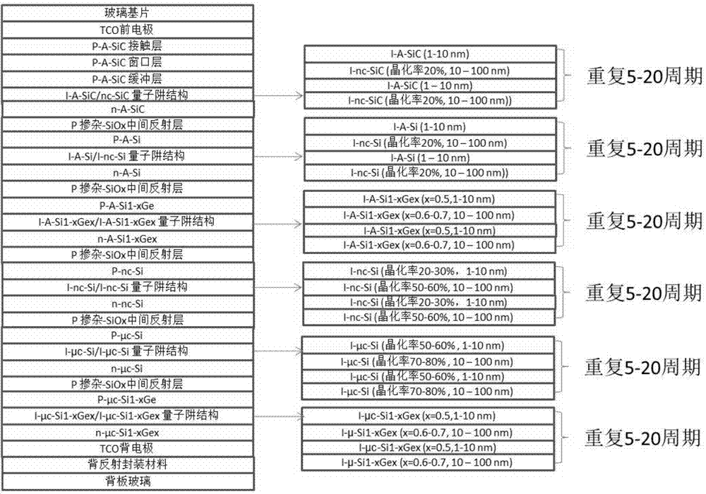
[0044] For multi-junction silicon-based thin-film solar cells with quantum well structure, figure 1 It is a structural diagram of a multi-junction silicon-based thin film solar cell with a quantum well structure; its quantum well structure is formed by matching and combining the following materials: amorphous SiC (2.1-2.3eV) / nanocrystalline SiC (1.8-2.1eV), amorphous Si (1.7eV) / nanocrystalline Si (1.7eV to 1.2eV), amorphous Si1-xGex (0≤X≤1, 1.7eV to 1.2eV) / amorphous Si1-xGex (0≤X≤1, 1.5eV to 1.2eV), nanocrystalline Si (1.2eV to 1.7eV) / nanocrystalline Si (1.1eV to 1.5eV), nanocrystalline Si (1.1eV to 1.5eV) / microcrystalline Si (1.1eV).
[0045] Such as Figure 4 As shown, the manufacturing method of the silicon-based thin-film solar cell with quantum well structure comprises:
[0046] (1) cleaning the glass substrate;
[0047] (2) preparing the TCO front electrode on the substrate;
[0048] (3) Using a 355nm wavelength laser to divide the front electrode of the TCO to form ...
Embodiment 2
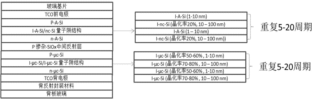
[0069] For double-junction silicon-based thin-film solar cells, figure 2 It is a schematic diagram of the structure of an amorphous / microcrystalline double-junction silicon-based thin-film solar cell with a quantum well structure; its quantum well structure is formed by a matching combination of the following materials, amorphous Si (1.7eV) / nanocrystalline Si (1.7eV to 1.2eV) , nanocrystalline Si (1.2eV to 1.7eV) / nanocrystalline Si (1.1eV to 1.5eV) and amorphous Si (1.7eV) / nanocrystalline Si (1.7eV to 1.2eV), nanocrystalline Si (1.2eV to 1.5 eV) / microcrystalline Si (1.1eV); and prepare multi-junction thin film solar cells with quantum well structure in descending order of energy level. Usually the thickness of the high energy gap material is 1-10nm, the thickness of the low energy gap material is 10-100nm, and the structural period of the quantum well is 5-20. In order to reduce the resistance of the quantum well, the thin film material in the quantum well structure is prope...
Embodiment 3
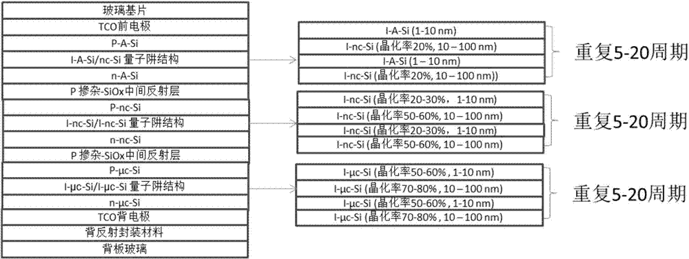
[0087] For triple-junction silicon-based thin-film solar cells, image 3It is a schematic diagram of the structure of an amorphous / microcrystalline / microcrystalline triple-junction silicon-based thin-film solar cell with a quantum well structure; its quantum well structure is formed by matching and combining the following materials: amorphous Si (1.7eV) / nano-Si (1.2eV to 1.7 eV), high-energy nanocrystalline Si (1.2eV to 1.7eV) / nanocrystalline Si (1.1eV to 1.5eV), nanocrystalline Si (1.1eV to 1.5eV) / microcrystalline Si (1.1eV). And prepare multi-junction thin film solar cells with quantum well structure in descending order of energy level. Usually the thickness of the high energy gap material is 1-10nm, the thickness of the low energy gap material is 10-100nm, and the structural period of the quantum well is 5-20. In order to reduce the resistance of the quantum well, the thin film material in the quantum well structure is properly doped with phosphorus (P) and boron (B), and ...
PUM
| Property | Measurement | Unit |
|---|---|---|
| Thickness | aaaaa | aaaaa |
| Thickness | aaaaa | aaaaa |
| Band gap width | aaaaa | aaaaa |
Abstract
Description
Claims
Application Information