Transistor forming method

一种晶体管、工艺的技术,应用在半导体制造领域,能够解决晶体管抑制漏电流的能力有限等问题,达到提高载流子迁移率、减少漏电流、厚度均匀的效果

Active Publication Date: 2015-07-01
SEMICON MFG INT (SHANGHAI) CORP
View PDF5 Cites 5 Cited by
  • Summary
  • Abstract
  • Description
  • Claims
  • Application Information

AI Technical Summary

Problems solved by technology

[0005] However, in prior art transistors with stressed layers, the improvement of carrier mobility in the channel region is limited, and the ability of the transistor to suppress leakage current is limited.

Method used


Image

  • Transistor forming method
  • Transistor forming method
  • Transistor forming method

Examples


Embodiment Construction

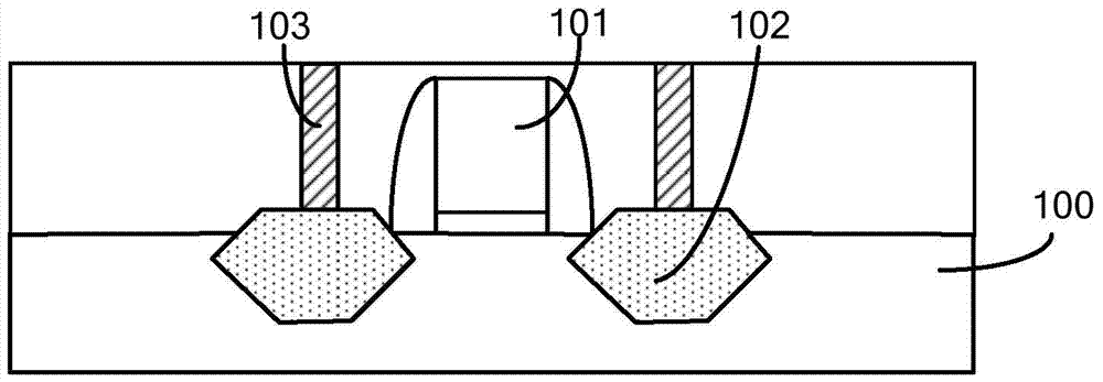
[0032] As mentioned in the background, in the existing transistors with the stress layer, the carrier mobility in the channel region is limited to increase, so the ability of the transistor to suppress the leakage current is limited.

[0033] After research, please continue to refer to figure 1 , the material of the stress layer 102 has a lattice structure, so there are lattice gaps in the stress layer 102 . Especially for NMOS transistors, the material of the stress layer 102 is silicon carbide, and the lattice constant of the silicon carbide is small, that is, the stress layer 102 has a small lattice size and a large lattice gap. The larger lattice gap will trap N-type or P-type dopant ions in the source region or the drain region, resulting in a reduction in the activation amount of the dopant ions after the dopant ions in the source region and the drain region are activated. When the doping ions activated by the source region or the drain region decrease, the resistance of ...


PUM

PropertyMeasurementUnit
energyaaaaaaaaaa
doping levelaaaaaaaaaa
energyaaaaaaaaaa

Abstract

Various embodiments provide transistors and methods for forming the same. In an exemplary method, a substrate can be provided. A gate structure can be formed on the substrate. A stress layer can be formed in the substrate on both sides of the gate structure. Barrier ions can be doped in the stress layer to form a barrier layer in the stress layer. The barrier layer can have a preset distance from a surface of the stress layer. An electrical contact layer can be formed using a portion of the stress layer on the barrier layer by a salicide process. The electrical contact layer can contain a first metal element. The first metal element can have a resistivity lower than a resistivity of a silicidation metal. The barrier layer can prevent atoms of the first metal element from diffusing to a bottom of the stress layer.

Description

technical field [0001] The invention relates to the technical field of semiconductor manufacturing, in particular to a method for forming a transistor. Background technique [0002] With the rapid development of semiconductor manufacturing technology, semiconductor devices are developing towards higher component density and higher integration. Transistors are currently being widely used as the most basic semiconductor devices, so as the element density and integration of semiconductor devices increase, the gate size of transistors has become shorter than before. However, the shortening of the gate size of the transistor will cause the short-channel effect of the transistor, thereby generating leakage current, and ultimately affecting the electrical performance of the semiconductor device. At present, the prior art mainly improves the performance of semiconductor devices by increasing carrier mobility. When the mobility of carriers is increased, the driving current of the t...

Claims


Application Information

Patent Timeline
Patent Type & Authority Applications(China)
IPC IPC(8): H01L21/336
CPCH01L21/02529H01L29/665H01L29/495H01L21/324H01L21/26513H01L21/0262H01L29/7848H01L21/30604H01L29/165H01L29/456H01L21/02636H01L21/2254H01L29/1608H01L29/0607H01L29/66477H01L21/26506H01L29/45H01L29/66628H01L29/66636H01L21/30608H01L21/3065H01L21/28518H01L29/1054H01L29/1083H01L2924/13091
Inventor 周祖源
Owner SEMICON MFG INT (SHANGHAI) CORP
Why Eureka
Try Eureka