Method for preparing ordered germanium quantum dot on silicon substrate by sputtering

A technology of silicon substrate and quantum dots, which is applied in the field of semiconductor quantum material preparation, achieves the effect of low cost and simple process

Inactive Publication Date: 2015-07-08
YUNNAN UNIV
View PDF9 Cites 10 Cited by
  • Summary
  • Abstract
  • Description
  • Claims
  • Application Information

AI Technical Summary

Problems solved by technology

However, after searching the literature, there is no report on the self-organized growth of germanium quantum d

Method used


Image

  • Method for preparing ordered germanium quantum dot on silicon substrate by sputtering
  • Method for preparing ordered germanium quantum dot on silicon substrate by sputtering
  • Method for preparing ordered germanium quantum dot on silicon substrate by sputtering

Examples


Embodiment 1

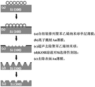
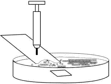
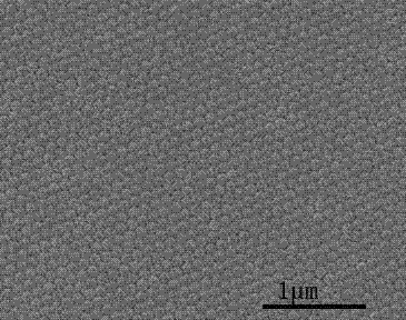
[0027] The sputter growth equipment used is FJL560 In the ion beam sputtering chamber of the type ultra-high vacuum multi-target magnetron and ion beam combined sputtering equipment, a Kaufman ion gun is placed in the growth chamber; the target used is 5N (99.999%) high-purity Ge square target and high Pure Si square target, the sputtering gas is 5N (99.999%) high-purity argon gas; the equipment used for sputtering Au is SCD005 ion sputtering instrument, and the target material is 99.99% high-purity Au circular target; the Si substrate used A P-type single-crystal Si wafer with a crystal orientation of (100) is used, polished on one side, and the resistivity is 1 Ω cm to 2 Ω cm; the commercially available polystyrene nanospheres have a mass percentage of 1% and a diameter of 100 nm ; The glass slides purchased are sailboat brand glass slides; the utensils are plastic watch glasses; ultrasonic cleaning uses a commercially available ultrasonic cleaner. Specific steps are as fo...

Embodiment 2

[0040] The equipment and materials used are all the same as in Example 1. The specific steps are:

[0041] 1. Preparation of two-dimensional ordered hexagonal nanopit pattern:

[0042] Same as Example 1.

[0043] 2. Preparation of ordered Ge quantum dots by ion beam sputtering technology:

[0044] A. Use the improved RCA cleaning method to clean the silicon substrate etched by polystyrene nanospheres; after cleaning, dry the silicon substrate with high-purity nitrogen, put it into the ion beam sputtering chamber, and wait for the background vacuum of the sputtering chamber degree less than 3.0×10 -4 Pa, adjust the temperature to 800 °C and keep it for 10 min; then fill the sputtering chamber with argon with a purity of 5N as the working gas, and adjust the pressure to 2.0×10 -2 Pa;

[0045] B. At 800 ℃, the discharge voltage is 75 V, the beam voltage is 0.5 KV, the acceleration voltage is 200 V, the growth beam current is 4 mA, and the sputtering rate is 0.1 ? / s. The b...


PUM

PropertyMeasurementUnit
Resistivityaaaaaaaaaa
Diameteraaaaaaaaaa
The average diameteraaaaaaaaaa

Abstract

The invention relates to a method for preparing an ordered germanium quantum dot on a silicon substrate by sputtering and belongs to the technical field of semiconductor quantum material. The method comprises the following steps: preparing a two-dimensional ordered hexagonal nano-pit pattern on the surface of the silicon substrate through a polrvinyl benzene nanosphere corrosion technology, growing a silicon buffer layer on the patterned silicon substrate through an ion beam sputtering technology by taking high-purity argon as the working gas under the conditions that the base vacuum degree of a sputtering chamber is less than 3.0*10<-4> Pa, the growth temperature is 400-800 DEG C, the beam voltage is 0.5-1.1 KV and the growth beam is 4-15 mA; and performing self-organized growth to form a single layer ordered germanium quantum dot. The method is a novel method for realizing the volume production of the quantum dot material with low cost, simple process and high production efficiency and provides a good method for researching an efficient quantum dot laser and even a nano-laser.

Description

technical field [0001] The invention relates to a method for preparing semiconductor quantum materials, in particular to a method for growing ordered germanium quantum dots from tissue by using ion beam sputtering technology on a silicon substrate etched by polystyrene nanospheres. Background technique [0002] Quantum dots, also known as artificial atoms, are a zero-dimensional quantum structure. When the particle size reaches the nanometer level, size confinement will cause size effects, quantum confinement, macroscopic quantum tunneling effects and surface effects. These unique quantum effects make Quantum dot materials are widely used in the research of optoelectronic information devices. In the past few decades, the development of silicon-based quantum dot devices has made amazing progress, and the microelectronics industry based on this has rapidly grown into one of the largest and most vital industries in the world. However, the self-organized growth of quantum dots ...

Claims


Application Information

Patent Timeline
IPC IPC(8): C23C14/18C23C14/34C23C14/02H01L21/02H01L21/203B82Y30/00B82Y40/00
Inventor 杨宇杨杰王茺邱锋王兆卿王海澎辛征航
Owner YUNNAN UNIV
Why Eureka
Try Eureka