Production method for semiconductor epitaxial wafer, semiconductor epitaxial wafer, and production method for solid-state imaging element

A technology for epitaxial wafers and manufacturing methods, which is applied in semiconductor/solid-state device manufacturing, semiconductor devices, electric solid-state devices, etc., can solve problems such as insufficiency, achieve high gettering ability, and inhibit metal pollution.

Active Publication Date: 2015-07-15
SUMCO CORP
View PDF11 Cites 6 Cited by
  • Summary
  • Abstract
  • Description
  • Claims
  • Application Information

AI Technical Summary

Problems solved by technology

In recent years, these metal contaminations have been improved to some extent by changing the constituent materials of the epitaxial growth furnace to materials with excellent corrosion resistance, etc., but this is not enough.

Method used


Image

  • Production method for semiconductor epitaxial wafer, semiconductor epitaxial wafer, and production method for solid-state imaging element
  • Production method for semiconductor epitaxial wafer, semiconductor epitaxial wafer, and production method for solid-state imaging element
  • Production method for semiconductor epitaxial wafer, semiconductor epitaxial wafer, and production method for solid-state imaging element

Examples


Embodiment

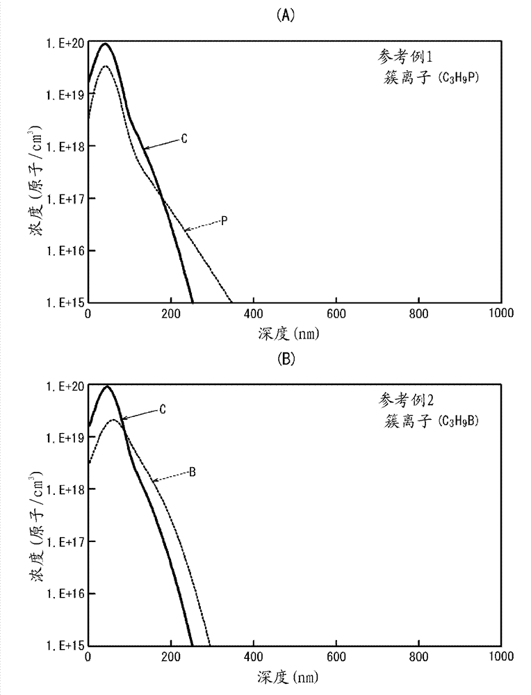
[0086] (Refer to the experimental example)

[0087] First, in order to clarify the difference between cluster ion irradiation and monomer ion implantation, the following experiments were performed.

reference example 1)

[0089] An n-type silicon wafer (diameter: 300 mm, thickness: 725 μm, doping: phosphorus, doping concentration: 5×10 14 atom / cm 3 ). Next, trimethylphosphine (C 3 h 9 P) ionization, at a carbon dose of 5.0 x 10 14 atom / cm 2 , Phosphorus dosage 1.7×10 14 atom / cm 2 The silicon wafer was irradiated under the conditions of an accelerating voltage of 12.8 keV / atom per carbon atom and an accelerating voltage of 32 keV / atom per phosphorus atom.

reference example 2)

[0091] For the same silicon wafer as in Reference Example 1, instead of trimethylphosphine, trimethylboron (C 3 h 9 B) As the material gas, cluster ions are generated, and the dose of boron is 1.7×10 14 atom / cm 2 The silicon wafer was irradiated under the same conditions as in Reference Example 1 except that the accelerating voltage per boron atom was 14.5 keV / atom.

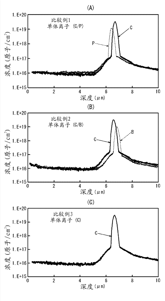
[0092] (reference example 3)

[0093] For the same silicon wafer as in Reference Example 1, instead of cluster ion irradiation, CO 2 As a material gas, carbon monomer ions are generated at a dose of 5.0×10 14 atom / cm 2 1. Under the condition of accelerating voltage 80keV / atom, the silicon wafer is implanted. Afterwards, phosphine trihydrogen (PH 3 ) as a material gas to generate phosphorous monomer ions at a dose of 1.7×10 14 atom / cm 2 1. Under the condition of accelerating voltage 80keV / atom, the silicon wafer is implanted.

[0094] (reference example 4)

[0095] For the same silicon wafer as in Refer...


PUM

PropertyMeasurementUnit
thicknessaaaaaaaaaa
thicknessaaaaaaaaaa
thicknessaaaaaaaaaa

Abstract

The present invention provides a production method for a semiconductor epitaxial wafer in which increased gettering properties enable metal contamination to be suppressed. In the present invention, the production method for the semiconductor epitaxial wafer is characterized in that the method includes: a first step, in which cluster ions (16) are irradiated on a surface (10A) of a semiconductor wafer (10) so as to form, on the surface (10A) of the semiconductor wafer, a modification layer (18) that is a solid solution of carbon and a dopant element, which are constituent elements of the cluster ions (16); and a second step in which an epitaxial layer (20), which has a lower dopant element concentration than the peak dopant element concentration in the modification layer (18), is formed upon the modification layer (18) of the semiconductor.

Description

technical field [0001] The present invention relates to a method for manufacturing a semiconductor epitaxial wafer, a method for manufacturing a semiconductor epitaxial wafer, and a solid-state imaging device. In particular, the present invention relates to a method of manufacturing a semiconductor epitaxial wafer capable of suppressing metal contamination by exerting higher gettering capability. Background technique [0002] Metal contamination is mentioned as a factor that degrades the characteristics of semiconductor devices. For example, in a back-illuminated solid-state imaging device, metal mixed into a semiconductor epitaxial wafer serving as a substrate of the device causes an increase in dark current of the solid-state imaging device, causing a defect called a white damage defect. The back-illuminated solid-state imaging device can directly introduce light from the outside to the sensor by arranging the wiring layer and the like on the lower layer than the sensor p...

Claims


Application Information

Patent Timeline
Patent Type & Authority Applications(China)
IPC IPC(8): H01L21/322C23C16/02C23C16/42C30B23/02H01L21/20H01L21/205H01L21/265H01L27/14
CPCH01L21/02381H01L27/14689H01L21/02579H01L21/26566H01L21/02532H01L21/26513H01L21/02658H01L21/3221H01L21/02576C23C14/48H01L21/26506H01L21/02439C30B25/186C30B29/06H01L21/2658H01L27/14687H01L21/324H01L29/167
Inventor 门野武栗田一成
Owner SUMCO CORP
Why Eureka
Try Eureka