Film transistor, array substrate and preparation method thereof, display device

A technology of thin-film transistors and array substrates, applied in the display field, can solve problems such as rising production costs, scarcity of indium elements, and reduction of indium elements

Active Publication Date: 2015-09-23
BOE TECH GRP CO LTD +1
View PDF4 Cites 4 Cited by
  • Summary
  • Abstract
  • Description
  • Claims
  • Application Information

AI Technical Summary

Problems solved by technology

[0005] Embodiments of the present invention provide a thin film transistor, an array substrate and its preparation method, and a display device, which can reduce the use of indium elements in the semiconductor active layer, thereby solving the problem of rising production costs due to the increasing scarcity of indium elements question

Method used


Image

  • Film transistor, array substrate and preparation method thereof, display device
  • Film transistor, array substrate and preparation method thereof, display device
  • Film transistor, array substrate and preparation method thereof, display device

Examples


preparation example Construction

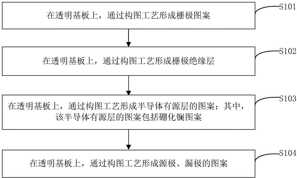
[0025] An embodiment of the present invention provides a method for preparing a thin film transistor, such as figure 1 As shown, can include:

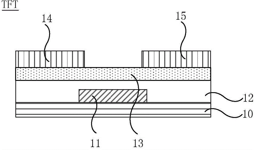
[0026] S101, such as Figure 2a As shown, on the transparent substrate 10, a gate pattern 11 is formed by a patterning process.

[0027] S102 , on the transparent substrate 10 , form a gate insulating layer 12 through a patterning process.

[0028] S103. On the transparent substrate 10, a pattern of the semiconductor active layer 13 is formed through a patterning process; wherein, the pattern of the semiconductor active layer 13 includes a lanthanum boride pattern.

[0029] S104 , on the transparent substrate 10 , forming patterns of the source electrode 14 and the drain electrode 15 through a patterning process.

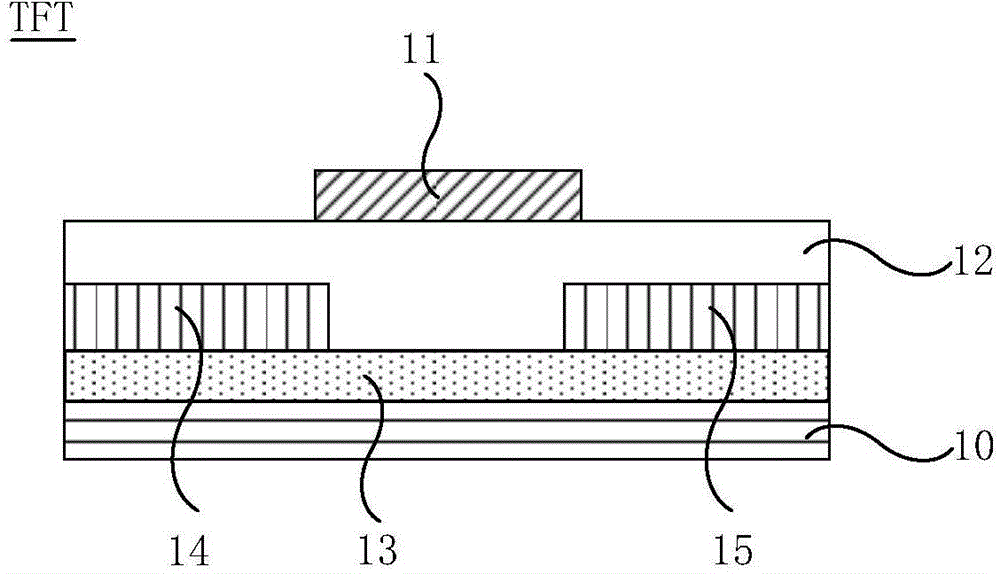
[0030] It should be noted that, first, the present invention does not limit the sequence of the above steps S101 to S104. For example when a TFT such as Figure 2a When the bottom-gate thin film transistor is shown, the...

Embodiment 1

[0043] The preparation method provided in this embodiment is used to prepare such as Figure 2a The shown TFT, especially the semiconductor active layer 13 mainly composed of lanthanum boride, is prepared by physical vapor deposition in this embodiment, as image 3 As shown, the method for preparing TFT may include:

[0044] S201 , forming a pattern of the gate 11 on the transparent substrate 10 .

[0045] Specifically, on the transparent substrate 10, a gate metal layer with a thickness of 100 nm-2000 nm is prepared by physical vapor deposition. Wherein, the gate metal layer can be made of metal, metal alloy or conductive metal oxide. It can also be composed of more than two layers of conductive materials, such as two layers of molybdenum metal layers and an aluminum metal layer between the two layers of molybdenum metal layers, that is, Mo / Al / Mo (molybdenum / aluminum / molybdenum) and the like. Then, apply photoresist on the surface of the gate metal layer, and use a common ...

Embodiment 2

[0060] The preparation method provided in this embodiment is used to prepare such as Figure 2a Shown TFT, described method specifically comprises:

[0061] Firstly, an Al thin film with a thickness of 300 nm is formed on the transparent substrate 10, and the pattern of the gate 11 is formed through masking, exposure, etching and developing processes.

[0062] Next, a gate insulating layer 12 with a thickness of 200 nm is prepared by anodic oxidation on the substrate on which the pattern of the gate 11 is formed.

[0063] Next, on the substrate on which the gate insulating layer 12 is formed, a lanthanum boride film layer is prepared by sputtering.

[0064] Specifically, the lanthanum boride target is first installed on the sputtering apparatus, and a thin film is prepared by direct sputtering. During the sputtering process, the preparation pressure is controlled to be 0.3Pa, and the growth rate of the film is 10nm / min to form a thick film. 20nm lanthanum boride thin film la...


PUM

PropertyMeasurementUnit
thicknessaaaaaaaaaa
thicknessaaaaaaaaaa
thicknessaaaaaaaaaa

Abstract

The invention embodiment provides a film transistor, an array substrate and a preparation method thereof, and a display device, and relates to the display technical field; indium element in an active layer of a semiconductor can be reduced in usage, thus solving the rising making cost problems caused by rareness of the indium element; the film transistor preparation method comprises the following steps: using composition technology to form a semiconductor active layer pattern on a transparent substrate, wherein the semiconductor active layer pattern comprises a lanthanum boride pattern.

Description

technical field [0001] The invention relates to the field of display technology, in particular to a thin film transistor, an array substrate and a preparation method thereof, and a display device. Background technique [0002] Thin Film Transistor (TFT for short) is one of the most important electronic devices in the field of display technology, used to control and drive Liquid Crystal Display (LCD for short) and Organic Light Emitting Diode (OLED for short) ) sub-pixels of the display. [0003] With the rapid development of display technology, thin film transistor technology has developed from the original a-Si (amorphous silicon) thin film transistor to the current LTPS (low temperature polysilicon) thin film transistor, MILC (metal induced lateral crystallization) thin film transistor, oxide (oxidation objects) thin film transistors, etc. Oxide thin film transistors, which are widely used at present, use oxide semiconductor as the active layer, which has the characteris...

Claims


Application Information

Patent Timeline
Patent Type & Authority Applications(China)
IPC IPC(8): H01L29/786H01L29/24H01L29/66
CPCH01L29/24H01L29/66969H01L29/78603H01L29/66H01L29/66742H01L29/78681H01L29/7869H01L29/78696H01L21/02565H01L21/02631H01L27/1225H01L27/127H01L27/1288
Inventor 袁广才闫梁臣徐晓光王磊彭俊彪兰林锋
Owner BOE TECH GRP CO LTD
Why Eureka
Try Eureka