Multi-layer heterogeneous antireflection film solar cell

A technology of solar cells and anti-reflection coatings, applied in circuits, photovoltaic power generation, electrical components, etc., can solve the problems of adverse effects on cell conversion efficiency, inability to be effectively used, and easy breakage, and achieve excellent PID-Free performance and improve Effects of improving physical properties, electrical properties, and photoelectric conversion efficiency

Inactive Publication Date: 2015-09-30
HENGDIAN GRP DMEGC MAGNETICS CO LTD
View PDF4 Cites 9 Cited by
  • Summary
  • Abstract
  • Description
  • Claims
  • Application Information

AI Technical Summary

Problems solved by technology

2. Electrical loss, which includes the recombination of photogenerated carriers on the surface of semiconductors and in the body, the bulk resistance of semiconductors and metal grid lines, and the loss of metal-semiconductor contact resistance
[0003] The role of the anti-reflection film in conventional crystalline silicon solar technology is to reduce optical loss and passivate the surface of the battery. The current mainstream anti-reflection film is a single-structure SiNx:H film. This single-structure SiN:H film has the following disadvantages: 1 ) The dielectric constant is low, and the anti-PID performance is poor; 2) In terms of optical properties, the extinction coefficient is high, and some photons are absorbed and consumed by the SiNx: H film, which cannot be effectively used; 3) SiNx: H film is exposed to ultraviolet light during the annealing process. The lower Si-H bond is easily broken, resulting in the escape of H, which makes the surface passivation effect worse, and the conversion efficiency of the cell is adversely affected

Method used


Image

  • Multi-layer heterogeneous antireflection film solar cell
  • Multi-layer heterogeneous antireflection film solar cell
  • Multi-layer heterogeneous antireflection film solar cell

Examples


Embodiment 1

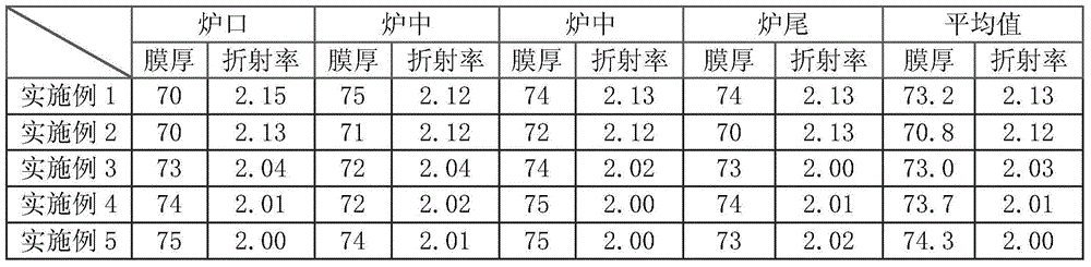
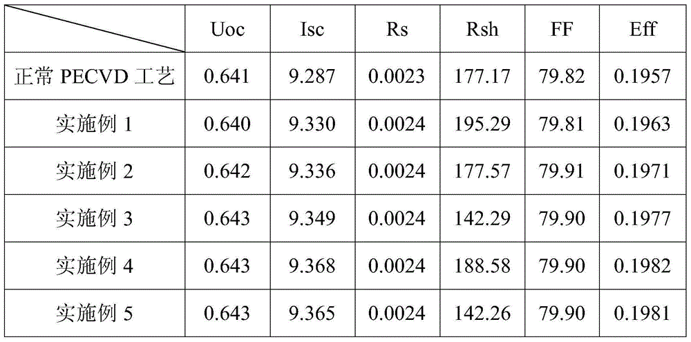
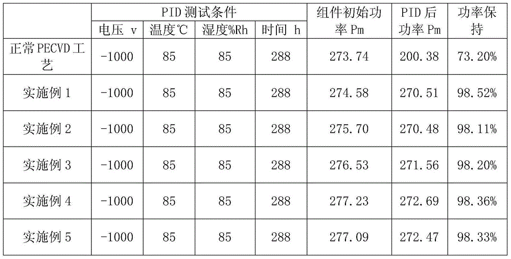
[0024] Put the 156.75mm*205mm silicon wafer after etching and cleaning into the PECVD furnace tube, and deposit the following films in sequence according to the steps: the first step is SiO 2Membrane → second step SiN x Membrane → third step SiO x N y Membrane → Step 4 SiO 2 membrane. Wherein the first step process parameter is: N 2 O flow 4000sccm, SiH 4 The flow rate is 500sccm, the RF power is 3000W, the reaction pressure is 1500mT, the time is 200 seconds, and the temperature is 450 degrees; the process parameters of the second step are: SiH 4 The flow rate is 800sccm, NH 3 The flow rate is 5000sccm, the radio frequency power is 4000W, the reaction pressure is 1700mT, the time is 300 seconds, and the temperature is 450 degrees; the process parameters of the third step are: N 2 O flow 3000sccm, SiH 4 The flow rate is 500sccm, NH 3 The flow rate is 1000sccm, the radio frequency power is 3000W, the reaction pressure is 1500mT, the time is 100 seconds, and the tempera...

Embodiment 2

[0026] Put the 156.75mm*205mm silicon wafer after etching and cleaning into the PECVD furnace tube, and deposit the following films in sequence according to the steps: the first step is SiO 2 Membrane → second step SiN x Membrane → third step SiO x N y Membrane → Step 4 SiO 2 membrane. Wherein the first step process parameter is: N 2 O flow 4000sccm, SiH 4 The flow rate is 500sccm, the RF power is 3000W, the reaction pressure is 1500mT, the time is 100 seconds, and the temperature is 450 degrees; the process parameters of the second step are: SiH 4 The flow rate is 800sccm, NH 3 The flow rate is 5000sccm, the radio frequency power is 4000W, the reaction pressure is 1700mT, the time is 400 seconds, and the temperature is 450 degrees; the process parameters of the third step are: N 2 O flow 3000sccm, SiH 4 The flow rate is 500sccm, NH 3 The flow rate is 1000sccm, the radio frequency power is 3000W, the reaction pressure is 1500mT, the time is 100 seconds, and the temper...

Embodiment 3

[0028] Put the 156.75mm*205mm silicon wafer after etching and cleaning into the PECVD furnace tube, and deposit the following films in sequence according to the steps: the first step is SiO 2 Membrane → second step SiN x Membrane → third step SiO x N y Membrane → Step 4 SiO 2 membrane. Wherein the first step process parameter is: N 2 O flow 4000sccm, SiH 4 The flow rate is 500sccm, the RF power is 3000W, the reaction pressure is 1500mT, the time is 100 seconds, and the temperature is 450 degrees; the process parameters of the second step are: SiH 4 The flow rate is 600sccm, NH 3 The flow rate is 6000sccm, the radio frequency power is 4000W, the reaction pressure is 1700mT, the time is 400 seconds, and the temperature is 450 degrees; the process parameters of the third step are: N 2 O flow 3000sccm, SiH 4 The flow rate is 500sccm, NH 3 The flow rate is 1000sccm, the radio frequency power is 3000W, the reaction pressure is 1500mT, the time is 100 seconds, and the temper...


PUM


Abstract

The invention discloses a multi-layer heterogeneous antireflection film solar cell. The specific operation steps are: (1) adopting the conventional texturing, diffusing and etching processes; (2) on the basis of the conventional PECVD coating technology, after diffusing and etching, depositing a multi-layer heterogeneous antireflection film on the surface of a silicon wafer, wherein the multi-layer heterogeneous antireflection film has a structure of SiO2 / SiNx / SiOxNy / SiO2; (3) adopting the conventional process to print an electrode and conduct sintering, thereby obtaining the solar cell. The invention has the beneficial effects that the multi-layer heterogeneous antireflection film structure increases a dielectric constant of the antireflection film, reduces reflection of sunlight by the solar cell and reduces an extinction coefficient of the antireflection film. Meanwhile, the antireflection film achieves relatively good passivation effect, thereby enhancing physical and electrical properties of the solar cell. The crystalline-silicon solar cell of the invention has excellent PID-Free performance, and the photoelectric conversion efficiency is significantly improved.

Description

technical field [0001] The invention relates to the technical field related to the development of high-efficiency solar cell technology, in particular to a multilayer heterogeneous anti-reflection film solar cell. Background technique [0002] With the continuous maturity of crystalline silicon solar cell technology, it has become one of the main means to reduce production costs with high-efficiency cells to obtain higher energy to replace low-efficiency cells. Therefore, high-efficiency monocrystalline cell technology has also become a hot topic in scientific research. Great achievements have been made, and the conversion efficiency of high-efficiency batteries commercialized in the United States, Germany and Japan exceeds 20%. The research results show that there are currently two main reasons restricting the further improvement of the conversion efficiency of crystalline silicon solar cells: 1. Optical loss, including the reflection loss of the front surface of the cell, ...

Claims


Application Information

Patent Timeline
Patent Type & Authority Applications(China)
IPC IPC(8): H01L31/0216H01L31/18
CPCH01L31/02168H01L31/1804Y02E10/547Y02P70/50
Inventor 孙涌涛彭兴胡玉婷董方
Owner HENGDIAN GRP DMEGC MAGNETICS CO LTD
Why Eureka
Try Eureka