CMOS fully digital frequency adjustable pulse radio ultra-wideband transmitter

A pulsed radio and all-digital technology, applied in electrical components, transmission systems, etc., can solve problems such as large chip area and cost, waveform distortion, and incompatibility of CMOS processes, and achieve increased utilization, low power consumption, and simple structure. Effect

Active Publication Date: 2015-10-07
GUILIN UNIV OF ELECTRONIC TECH
View PDF4 Cites 5 Cited by
  • Summary
  • Abstract
  • Description
  • Claims
  • Application Information

AI Technical Summary

Problems solved by technology

At present, many literatures have been researched on IR-UWB transmitters. These UWBs are mainly realized by the following schemes: Scheme 1 is to first use a digital circuit to delay to obtain a narrow pulse. After the narrow pulse passes through the shaping network, the spectrum is moved to the required frequency band. , this scheme needs to use a large number of capacitors, inductors and resistors, so the chip area and cost are relatively large; the second scheme is to use the delay of the digital circuit to generate several narrow pulses, and then synthesize these narrow pulses into a frequency spectrum to meet The required pulse waveform, this scheme has very strict requirements on the waveform synthesis part, the waveform obtained will be completely distorted if the pulse synthesis time is slightly deviated; in addition, there is another scheme that uses the step recovery characteristics of the avalanche diode to obtain the required The narrow pulse signal of this scheme is not suitable for CMOS chip integration because the process of the avalanche diode device used is not compatible with the standard CMOS process.

Method used


Image

  • CMOS fully digital frequency adjustable pulse radio ultra-wideband transmitter
  • CMOS fully digital frequency adjustable pulse radio ultra-wideband transmitter
  • CMOS fully digital frequency adjustable pulse radio ultra-wideband transmitter

Examples


Embodiment Construction

[0024] The present invention will be further described below in conjunction with accompanying drawing:

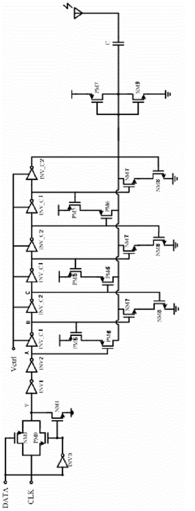
[0025] CMOS all-digital frequency tunable pulsed radio UWB transmitter, such as figure 1 As shown, it is mainly composed of OOK (binary on-off keying) modulation circuit, integer circuit, delay network, pulse sequence generation network, inverter and antenna.

[0026] The main function of the OOK modulation circuit is to process the input digital signal DATA and the clock signal CLK to generate a digital signal that meets the OOK modulation requirements. That is, when the digital signal DATA is at a high level "1", the output signal Y is the clock signal CLK, and when the digital signal DATA is at a low level "0", the output signal Y is "0".

[0027] The OOK modulation circuit is composed of NMOS transistors NM0, NM1, PMOS transistor PM0 and an inverter INV0 circuit. After the drain of the NMOS transistor NM0 is connected to the source of the PMOS transistor PM0, an input...


PUM


Abstract

The invention discloses a CMOS fully digital frequency adjustable pulse radio ultra-wideband transmitter, which includes an OOK modulation circuit, a time-delay network, a pulse sequence generation network and an antenna. The OOK modulation circuit processes an input digital signal DATA and a clock signal CLK, and generates a digital signal that meets the requirements of OOK modulation. On the basis of the time-delay characteristics of an inverter, the time-delay network makes a time-delay interval between an input signal and an output signal serve as an input signal of a subsequent pulse sequence generation network, and generates monopulse units with the same time width during the time-delay interval. Each monopulse signal generation circuit of the pulse sequence generation network generates a monopulse signal, pulse signals generated by all the monopulse signal generation circuits are combined to form a pulse sequence, and the whole pulse sequence is output by serving as an output signal and is emitted by the antenna. The pulse frequency of the transmitter is adjustable, and the work bandwidth meets UWB protocol requirements.

Description

technical field [0001] The invention relates to the technical field of pulse radio ultra-wideband, in particular to a CMOS all-digital frequency-adjustable pulse radio ultra-wideband transmitter. Background technique [0002] Since the U.S. Federal Communications Commission (FCC) promulgated the Ultra-Wideband (UWB) spectrum specification in 2002, and used the 3.1GHz-10.6GHz frequency band as an unlicensed frequency band for civilian UWB equipment, Ultra-Wideband Broadband communication technology has been applied research and attention in fields such as wireless personal area network, wireless sensor network, and biomedicine because of its simple system structure, high transmission rate, and low power consumption. [0003] Current UWB communication systems can be divided into three categories: Direct Sequence Spread Spectrum (DS-SS), Multiband Orthogonal Frequency Division Multiplexing (MB-OFDM), and Impulse Radio (IR). Among them, IR-UWB technology mainly uses a series of...

Claims


Application Information

Patent Timeline
Patent Type & Authority Applications(China)
IPC IPC(8): H04B1/7176H04B1/7163H04B1/40
Inventor 韦保林陈田徐卫林韦雪明段吉海
Owner GUILIN UNIV OF ELECTRONIC TECH
Why Eureka
Try Eureka