
A non-annealing perovskite solar cell and its preparation method

A solar cell and perovskite type technology, applied in the field of solar cells, can solve the problems of reducing the crystallization activation energy of perovskite thin films, complicated process and high cost, and achieve the effects of convenient industrial production, easy repetition and low preparation temperature

Active Publication Date: 2017-08-25
SUZHOU UNIV
View PDF4 Cites 0 Cited by
  • Summary
  • Abstract
  • Description
  • Claims
  • Application Information

AI Technical Summary

Problems solved by technology

[0005] Technical problem to be solved: conventional perovskite solar cells need an annealing process during the preparation process, which is complicated and costly. In order to simplify this process, the purpose of the present invention is to disclose a perovskite solar cell that does not require annealing. Mineral solar cell and its preparation method. The preparation method of the present invention reduces the activation energy of perovskite film crystallization by doping new materials during the preparation process of the perovskite layer film, so that it can be directly formed in the spin coating process without Annealing

Method used


Image

  • A non-annealing perovskite solar cell and its preparation method
  • A non-annealing perovskite solar cell and its preparation method
  • A non-annealing perovskite solar cell and its preparation method

Examples


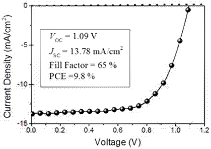
Embodiment 1

[0025] (1) Provide an ITO glass substrate and perform standardized cleaning;

[0026] (2) Methylammonium iodide (MAI) and lead chloride (PbCl 2 ) and indium chloride (InCl 3 ) was dissolved in the DMF solution at a molar ratio of 3:1:0.3, and stirred for 5 hours to obtain a 30wt% perovskite DMF solution;

[0027] (3) Spin-coat the PEDOT:PSS solution on the transparent electrode of the substrate, accelerate to 4500rpm and rotate for 40 seconds to form a uniform anode modification layer, and anneal at 100°C for 20 minutes;

[0028] (4) Process the perovskite layer film on the PEDOT:PSS film by spin coating method, accelerate to 4000rpm and rotate for 40 seconds, and disorderly annealing treatment can obtain a photosensitive layer with uniform crystallinity;

[0029] (5) The electron transport layer PCBM is processed by spin coating on the perovskite film, accelerated to 2000rpm and rotated for 40 seconds to obtain a uniform electron transport layer film;

[0030] (6) The cath...

Embodiment 2

[0032] (1) Provide an ITO flexible substrate and perform standardized cleaning;

[0033] (2) Methylammonium iodide (MAI) and lead chloride (PbCl 2 ) and indium chloride (InCl 3 ) was dissolved in the DMF solution at a molar ratio of 3:1:0.3, and stirred for 5 hours to obtain a 30wt% perovskite DMF solution;

[0034] (3) Spin-coat the PEDOT:PSS solution on the transparent electrode of the substrate, accelerate to 4500rpm and rotate for 40 seconds to form a uniform anode modification layer, and anneal at 100°C for 20 minutes;

[0035] (4) Process the perovskite layer film on the PEDOT:PSS film by spin coating method, accelerate to 4000rpm and rotate for 40 seconds, and disorderly annealing treatment can obtain a photosensitive layer with uniform crystallinity;

[0036] (5) The electron transport layer PCBM is processed by spin coating on the perovskite film, accelerated to 2000rpm and rotated for 40 seconds to obtain a uniform electron transport layer film;

[0037] (6) The c...

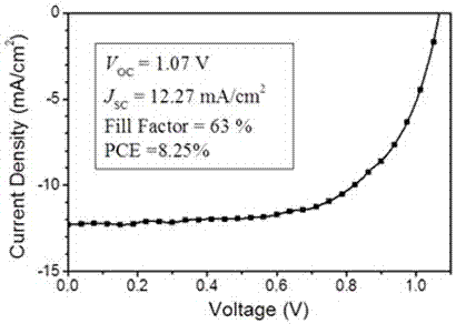
Embodiment 3

[0039] (1) Provide an ITO flexible substrate and perform standardized cleaning;

[0040] (2) Methylammonium iodide (MAI) and lead chloride (PbCl 2 ) and indium chloride (InCl 3 ) was dissolved in the DMF solution at a molar ratio of 3:1:0.25, and stirred for 2 hours to obtain a 30wt% perovskite DMF solution;

[0041] (3) Spin-coat the PEDOT:PSS solution on the transparent electrode of the substrate, accelerate to 4500rpm and rotate for 40 seconds to form a uniform anode modification layer, and anneal at 95°C for 40 minutes;

[0042] (4) Process the perovskite layer film on the PEDOT:PSS film by spin coating method, accelerate to 4000rpm and rotate for 40 seconds, and disorderly annealing treatment can obtain a photosensitive layer with uniform crystallinity;

[0043] (5) The electron transport layer PCBM is processed by spin coating on the perovskite film, accelerated to 2000rpm and rotated for 40 seconds to obtain a uniform electron transport layer film;

[0044] (6) The c...


PUM

PropertyMeasurementUnit
thicknessaaaaaaaaaa

Abstract

The invention belongs to the field of solar cells, and discloses a non-annealing perovskite solar cell and a preparation method thereof. In the preparation method, indium chloride is added to the perovskite precursor, and the method is spin-coated, soaked or pulled The thin film is obtained by the method, and the crystalline perovskite crystal is directly formed at room temperature, and then the electron transport layer is obtained by a non-annealing treatment method. The preparation method of the present invention adopts spin coating, inkjet printing or roll-to-roll printing method to process perovskite solar cells, has the advantages of simple preparation process, low preparation temperature, etc., and is conducive to greatly reducing the cost of organic solar cells; There are no strict requirements on the substrate, which is more conducive to the preparation of large-area, flexible and bendable devices; it avoids the status quo of poor repeatability of device efficiency caused by different degrees of crystallization during the annealing process of the perovskite layer, and the non-annealing process is simple and easy to repeat , improve the uniformity of device efficiency, and facilitate industrial production.

Description

technical field [0001] The invention belongs to the field of solar cells, and relates to a perovskite solar cell and a preparation method thereof, in particular to a non-annealing perovskite solar cell and a preparation method thereof. Background technique [0002] Perovskite solar cells are one of the research hotspots in the utilization of photovoltaic devices. Perovskite solar cells have attracted the attention of many researchers due to their low cost and simple structure. Its photoelectric conversion efficiency has rapidly increased from 3.8% to more than 15% in the past five years, and is favored by many scientific researchers. [0003] In 2009, Japanese researchers such as Miyasaka reported for the first time that organo-lead halides (CH3NH3PbBr3, CH3NH3PbI3) with a perovskite structure were used as photoelectric conversion materials for liquid electrolyte dye-sensitized solar cells. Due to the poor stability of the perovskite light-absorbing layer in the liquid ele...

Claims


Application Information

Patent Timeline
Patent Type & Authority Patents(China)
IPC IPC(8): H01L51/46H01L51/44H01L51/48H01L51/42
CPCH10K30/00H10K30/80Y02E10/549
Inventor 廖良生王照奎李萌
Owner SUZHOU UNIV
Learn More