Preparation method of novel light break-through IGBT device

A punch-through device technology, which is applied in the field of preparation of new light punch-through IGBT devices, can solve the problems of easily damaged IGBT devices, increased internal saturation current, and small short-circuit safe working area, so as to avoid large current impact, increase resistance value, The effect of ensuring the working life

Active Publication Date: 2015-11-11
四川广义微电子股份有限公司
View PDF4 Cites 11 Cited by
  • Summary
  • Abstract
  • Description
  • Claims
  • Application Information

AI Technical Summary

Problems solved by technology

like figure 1 The cell section of a second-generation light punch-through IGBT device is shown. Due to the combination of P+ type floating layer and N type carrier storage layer structure, the IGBT device can have high breakdown voltage and low forward conduction It has the advantages of low voltage drop and turn-off loss, but because the N-type carrier storage layer is thick (generally about 5 microns), the NN-type hole barrier formed with the N-substrate layer is therefore relatively high. Under the action of conductance modulation during on-time, a large number of holes will gather at the NN-junction, which will greatly increase the internal saturation current of the device. IGBT devices are easily damaged under impact

Method used


Image

  • Preparation method of novel light break-through IGBT device
  • Preparation method of novel light break-through IGBT device
  • Preparation method of novel light break-through IGBT device

Examples


Embodiment 1

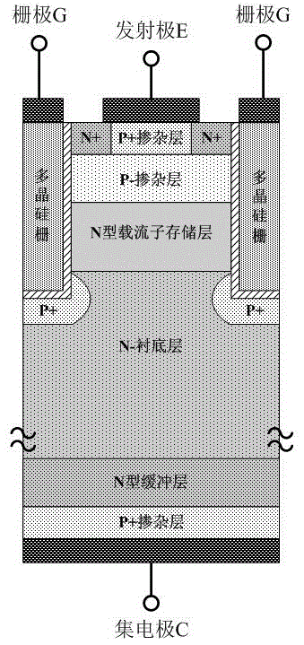
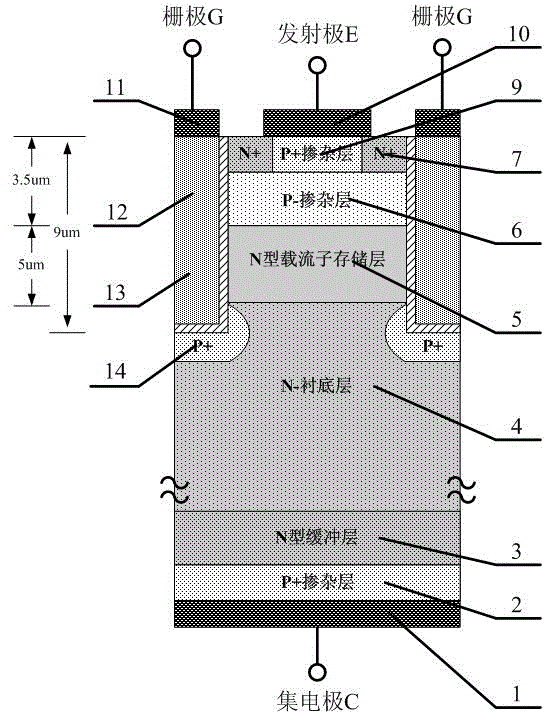
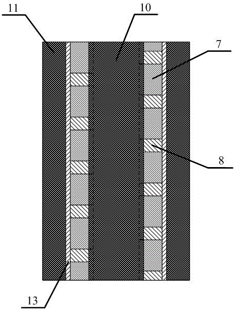
[0031] Embodiment one, figure 2 A schematic diagram of a cell section of the novel light punch-through IGBT device provided in this embodiment is shown, image 3 A schematic plan view of the cell plane of the novel light punch-through IGBT device provided in this embodiment is shown. The new light punch-through IGBT device includes several cells in a parallel structure, the lower surface of the cells is connected to the collector, and the collector metal contact layer 1, the first P+ doped layer 2, N type buffer layer 3 and N-substrate layer 4; the upper surface of the cell is respectively connected to the emitter and the gate, and the emitter metal contact layer 10 and the second P+ doped layer 9 are sequentially arranged below the emitter , a P-doped layer 6 and an N-type carrier storage layer 5, a gate metal contact layer 11, a trench gate structure composed of a polysilicon gate 12 and a gate oxide layer 13, and P+ type floating layer 14; the emitter metal contact layer...

Embodiment 2

[0038] Embodiment two, Figure 4 It shows the flow chart of the preparation method of the novel light punch-through IGBT device provided in this embodiment, Figure 5 It shows a schematic diagram of the cross section of the IGBT device shown in step S101 in the preparation method provided in this embodiment, Figure 6 It shows a schematic diagram of the cross section of the IGBT device shown in step S102 in the preparation method provided in this embodiment, Figure 7 It shows a schematic diagram of the section of the IGBT device shown in step S103 in the preparation method provided in this embodiment, Figure 8 It shows a schematic diagram of the section of the IGBT device shown in step S104 in the preparation method provided in this embodiment, Figure 9 It shows a schematic diagram of the section of the IGBT device shown in step S105 in the preparation method provided in this embodiment, Figure 10 It shows a schematic diagram of the cross section of the IGBT device show...


PUM


Abstract

The invention relates to the field of power semiconductor devices, and discloses a preparation method of a novel light break-through IGBT device. According to the IGBT device prepared by the preparation method, the structure of an N-type carrier storage layer and a P+ type floating layer is integrated, the IGBT device has advantages of high breakdown voltage, low forward conduction voltage drop and low turn-off loss, and the structure of N+ doping block layers and insulating block layers which are arranged in a staggered and spacing way side by side is arranged between a second P+ doping layer and a gate oxide layer so that the resistance value of an internal emission electrode integrated resistor can be greatly increased, increasing of internal saturation current can be effectively suppressed, the short circuit safe operating area of the IGBT device is expanded, and thus generation of high current impact can be avoided and the operating life of the device can be ensured.

Description

technical field [0001] The invention relates to the field of power semiconductor devices, in particular to a preparation method of a novel light punch-through IGBT device. Background technique [0002] IGBT (InsulatedGateBipolarTransistor, insulated gate bipolar transistor) is a composite fully controlled voltage composed of BJT (BipolarJunctionTransistor, bipolar transistor) and MOS (Metal-Oxid-Semicon-ductor, insulated gate field effect transistor) Driven power semiconductor devices combine the advantages of high input impedance of MOSFE (Metal-Oxide-SemiconductorField-Effect Transistor) and low conduction voltage drop of GTR (GiantTransistor, power transistor). The characteristics of small power and low saturation voltage are generally applicable to the conversion system with a DC voltage of 600V and above, such as AC motors, frequency converters, switching power supplies, lighting circuits, traction drives and other fields. [0003] In order to further tap the potential...

Claims


Application Information

Patent Timeline
Patent Type & Authority Applications(China)
IPC IPC(8): H01L29/66H01L29/06
CPCH01L29/063H01L29/0649H01L29/0684H01L29/66348
Inventor 张干王建全彭彪王作义崔永明
Owner 四川广义微电子股份有限公司
Why Eureka
Try Eureka