Low on-state loss insulated gate bipolar translator (IGBT) and manufacturing method thereof

A technology of on-state loss and manufacturing method, which is applied in the direction of semiconductor/solid-state device manufacturing, semiconductor devices, electrical components, etc., can solve the problems of poor safe working area and increased leakage, and reduce short-circuit current and on-state loss , Improve the effect of PIN area area

Active Publication Date: 2015-11-11
GLOBAL ENERGY INTERCONNECTION RES INST CO LTD +2
View PDF3 Cites 4 Cited by
  • Summary
  • Abstract
  • Description
  • Claims
  • Application Information

AI Technical Summary

Problems solved by technology

However, there are problems of increased leakage and poor safe working area under IGBT high voltage

Method used


Image

  • Low on-state loss insulated gate bipolar translator (IGBT) and manufacturing method thereof
  • Low on-state loss insulated gate bipolar translator (IGBT) and manufacturing method thereof
  • Low on-state loss insulated gate bipolar translator (IGBT) and manufacturing method thereof

Examples


Embodiment 1

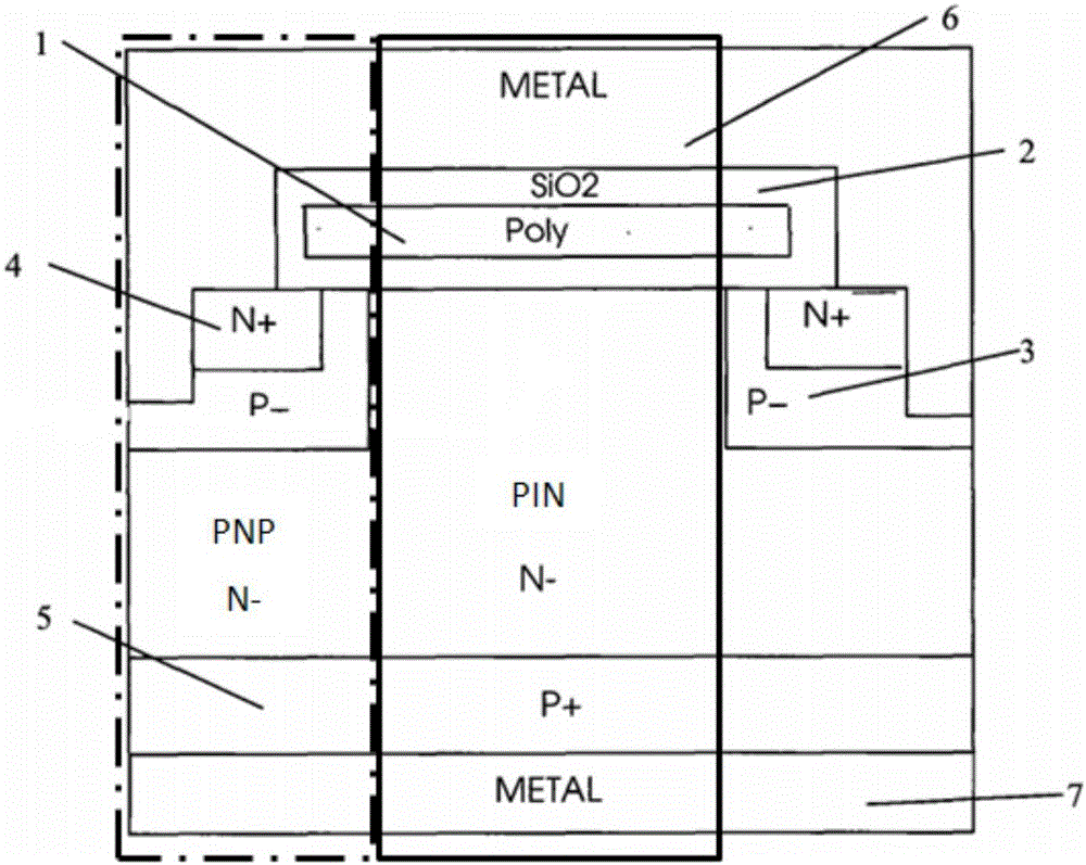
[0031] as attached Figure 4 As shown, the pattern of the pressure-resistant ring layer (PR) is changed, and the doping concentration of the P-base region is increased, so that the channel cannot be opened normally, and the channel becomes invalid. Empty cells are introduced in the IGBT active area. The left side of the graph is an empty cell structure, and the right side is a normal cell structure.

[0032] Preparation steps include:

[0033] 1) Preparation of the pressure-resistant ring layer (PR), including oxide layer growth, PR photolithography, PR implantation, and PR deglue;

[0034] 2) Active layer (OD) preparation, including field oxygen growth, OD photolithography, OD etching, and OD stripping;

[0035] 3) Preparation of polycrystalline layer (PS), including gate oxide growth, polycrystalline growth, polycrystalline doping, PS photolithography, PS etching, P well implantation, push junction, N+ source implantation, Spacer formation, anti-latch (latch -up) injecti...

Embodiment 2

[0041] as attached Figure 5 As shown, increasing the field oxygen layer (OD) pattern makes the channel current unable to be extracted and forms an empty cell structure in the IGBT active region. The left side of the graph is an empty cell structure, and the right side is a normal cell structure.

[0042] Preparation steps include:

[0043] 1) Active layer (OD) preparation, including field oxygen growth, OD photolithography, OD etching, and OD stripping;

[0044] 2) Preparation of polycrystalline layer (PS), including gate oxide growth, polycrystalline growth, polycrystalline doping, PS photolithography, PS etching, P well implantation, push junction, N+ source implantation, Spacer formation, anti-latch (latch -up) injection;

[0045] 3) Preparation of the contact layer (CO), including dielectric layer deposition, CO photolithography, CO etching, and CO debonding;

[0046] 4) Preparation of the metal layer (M1), including metal layer deposition, M1 photolithography, M1 cor...

Embodiment 3

[0050] as attached Image 6 As shown, changing the polycrystalline layer (PS) pattern, isolating the polycrystalline layer from the gate signal, forming polycrystalline islands, making the channel unable to open, and forming an empty cell structure in the IGBT active region. The left side of the graph is an empty cell structure, and the right side is a normal cell structure.

[0051] Preparation steps include:

[0052] 1) Active layer (OD) preparation, including field oxygen growth, OD photolithography, OD etching, and OD stripping;

[0053] 2) Preparation of polycrystalline layer (PS), including gate oxide growth, polycrystalline growth, polycrystalline doping, PS photolithography, PS etching, P well implantation, push junction, N+ source implantation, Spacer formation, anti-latch (latch -up) injection;

[0054] 3) Preparation of the contact layer (CO), including dielectric layer deposition, CO photolithography, CO etching, and CO debonding;

[0055] 4) Preparation of the...


PUM


Abstract

The invention provides a low on-state loss insulated gate bipolar translator (IGBT) and a manufacturing method thereof. The IGBT comprises an active region, a terminal region and a gate region, wherein the active region comprises an N-substrate region, a gate oxidation layer, a polycrystalline silicon gate, a P-base region, an N+ emitter region, a P+ collector region, emitter metal and collector metal; the active region is a cell region; a dummy cell structure is formed in the active region; the dummy cell structure is formed by sacrificing a cellular local channel; and the cellular local channel is sacrificed by changing one or combination of more of a pressure ring layer, a field oxide layer, a polycrystal layer and a contact hole layer. According to the manufacturing method provided by the invention, an invalid cell is introduced into the active region; the PIN / PNP region distribution of the active region is changed; the conductivity modulation effect of the cell of the IGBT is optimized; the saturation voltage of the IGBT is reduced; the current density of the IGBT is improved; and the on-state loss of the IGBT is reduced. The IGBT chip manufactured by the method has advantages in the field of high power density and low on-state loss application.

Description

technical field [0001] The invention belongs to the technical field of semiconductor devices, and in particular relates to a low on-state loss insulated gate bipolar transistor (IGBT) and a manufacturing method thereof. Background technique [0002] IGBT (Insulated Gate Bipolar Transistor) has the advantages of both unipolar devices and bipolar devices, simple driving circuit, low power consumption and cost of control circuit, low saturation voltage, low loss of the device itself, and is a mainstream device for high voltage and high current one. [0003] IGBT is a three-terminal device, including front emitter, gate and back collector. For the cross-sectional view of the active area of ​​the IGBT chip, see the attached figure 1 , including the emitter 6 on the front, the gate 1 and the collector 7 on the back. The surface is a MOSFET structure, and the back is a back-emitting P+ area. Among them: 1 polycrystalline, 2 oxide layer, 3P-base region, 4N+ emitter region, 5P+ c...

Claims


Application Information

Patent Timeline
Patent Type & Authority Applications(China)
IPC IPC(8): H01L29/739H01L21/331H01L29/06
CPCH01L29/0696H01L29/66333H01L29/7398
Inventor 刘江赵哿高明超王耀华何延强吴迪刘钺杨乔庆楠李晓平董少华金锐温家良
Owner GLOBAL ENERGY INTERCONNECTION RES INST CO LTD
Why Eureka
Try Eureka