Method for increasing conversion efficiency of thin-film solar cell

A solar cell and conversion efficiency technology, applied in circuits, electrical components, gaseous chemical plating, etc., can solve the problem that the surface of the N-type buffer layer cannot be completely covered, the conversion efficiency of thin-film solar cells is restricted, and the surface step coverage of the film layer is poor, etc. problem, to achieve the effect of improving photoelectric conversion efficiency, facilitating large-scale production, and good thickness consistency

Inactive Publication Date: 2015-11-11
GUANGDONG HANERGY THIN FILM SOLAR CO LTD
View PDF3 Cites 4 Cited by
  • Summary
  • Abstract
  • Description
  • Claims
  • Application Information

AI Technical Summary

Problems solved by technology

[0003] In the conventional preparation process, the intrinsic layer and the doped conductive layer are usually deposited by physical vapor deposition processes such as high-vacuum magnetron sputtering, and high-energy particles such as Ar ions during magnetron sputtering will bombard the film layer The surface of the N-type buffer layer is damaged, and the intrinsic layer and the doped conductive layer cannot completely cover the surface of the N-type buffer layer.
At the same time, the vacuum degree of the magnetron sputtering process is very high, ranging from 0.1Pa to 10Pa. Under this vacuum degree, the mean free path of the sputtered particles is long and the movement of the sputtered atoms is directional, which leads to the film layer The surface step coverage is poor, and the situation of preventing short circuit cannot be completely avoided; the coverage effect of the intrinsic layer and the doped conductive layer on the surface of the N-type buffer layer is further deteriorated, especially when the covered surface is stepped, the grain size is large, and the roughness It is especially obvious when the temperature is large, and accordingly, problems such as increased leakage current and decreased open circuit voltage have occurred, which restrict the improvement of the conversion efficiency of thin-film solar cells.

Method used


Image

  • Method for increasing conversion efficiency of thin-film solar cell
  • Method for increasing conversion efficiency of thin-film solar cell
  • Method for increasing conversion efficiency of thin-film solar cell

Examples


Embodiment Construction

[0023] In order to further understand the content of the present invention, the content of the invention and specific embodiments are specifically described below:

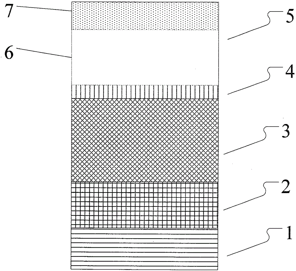
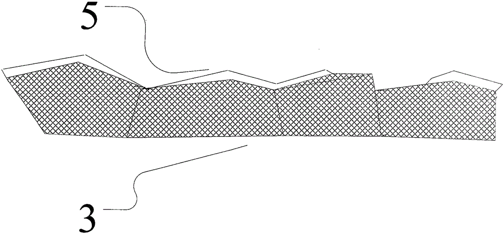
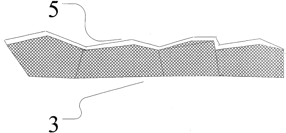
[0024] Such as figure 1 As shown, the thin-film solar cell includes a substrate 1, a back electrode 2, a P-type light absorbing layer 3, an N-type buffer layer 4 and a window layer 5, and the above-mentioned back electrode 2, P-type light absorbing layer 3, and N-type buffer layer 4 Depositing the window layer 5 and the window layer 5 on the substrate 1 sequentially is a method for improving the conversion efficiency of thin-film solar cells. Before processing the window layer 5, the semi-finished cell sheet to be processed is prepared first.

[0025] The production of semi-finished batteries can be processed according to the following methods according to the choice of glass or stainless steel for the substrate material:

[0026]When selecting glass as the substrate 1, first plate the back electrode 2 of the mol...


PUM

PropertyMeasurementUnit
thicknessaaaaaaaaaa

Abstract

The invention relates to the photovoltaic field of thin-film solar cells, and provides a method for increasing the conversion efficiency of a thin-film solar cell. The thin-film solar cell includes a substrate, a back electrode, a P-type light absorption layer, an N-type buffer layer and a window layer, wherein the back electrode, the P-type light absorption layer, the N-type buffer layer and the window layer are successively deposited on the substrate. The window layer includes an intrinsic layer and a doping conducting layer, the intrinsic layer is an intrinsic i-ZnO thin film, and the doping conducting laye ris aluminum-doping ZnO: AI thin film or a boron-doping ZnO:B thin film. The intrinsic layer and the doping conducting layer both have diethylzinc or dimethylzinc acting as zinc sources and are deposited to thin films by adopting a low pressure chemical vapor deposition method. The intrinsic layer and the doping conducting layer are successively deposited on the surface of the N-type buffer layer. The solar cell prepared by the method herein has the characteristics of high conversion efficiency, low requirements for technology and devices, easy mass-production and low cost.

Description

technical field [0001] The invention relates to the technical field of preparation of thin-film solar cells, in particular to a method for improving conversion efficiency of thin-film solar cells. Background technique [0002] Thin-film solar cells, especially copper indium gallium selenide (CIGS) thin-film solar cells, are favored by the photovoltaic industry all over the world for their low cost, high photoelectric conversion efficiency, no photodegradation effect, radiation resistance, wide spectral response range, and high cost performance. widespread attention. But at the same time, its structural characteristics and the characteristics of the multi-element materials involved are complex, with sensitive element ratio requirements and complex layered structure, and the process equipment technology is complicated. A typical metal compound thin film solar cell structure consists of a P-type light absorbing layer, an N-type buffer layer and a transparent conductive zinc ox...

Claims


Application Information

Patent Timeline
Patent Type & Authority Applications(China)
IPC IPC(8): H01L31/18C23C16/40
CPCY02P70/50
Inventor 汤安东蒿俊波
Owner GUANGDONG HANERGY THIN FILM SOLAR CO LTD
Why Eureka
Try Eureka