

Manufacturing method for high linear density EUV multilayer blazed grating
A technology of blazed gratings and multi-layer films, applied in the direction of diffraction gratings, optics, optical elements, etc., can solve the problems of low grating line density, low diffraction efficiency and low spectral resolution, increase the grating line density, and simplify complex processes , Improve the effect of diffraction efficiency and spectral resolution
- Summary
- Abstract
- Description
- Claims
- Application Information
AI Technical Summary
Problems solved by technology
Method used
Image

Examples
Embodiment 1
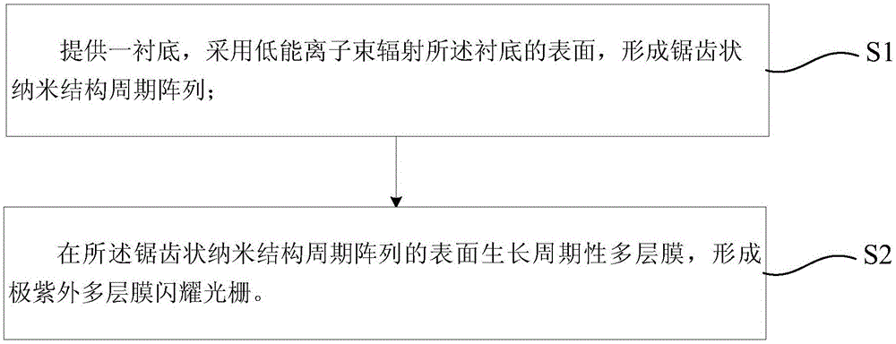
[0037] The invention provides a method for preparing a high linear density extreme ultraviolet multilayer film blazed grating, such as figure 1 As shown, the preparation method at least includes the following steps:
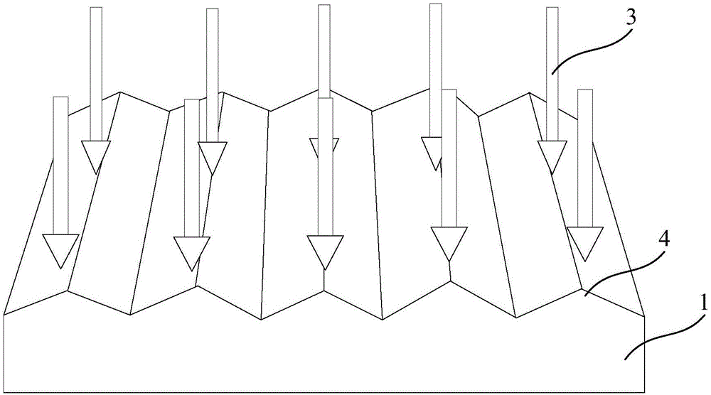
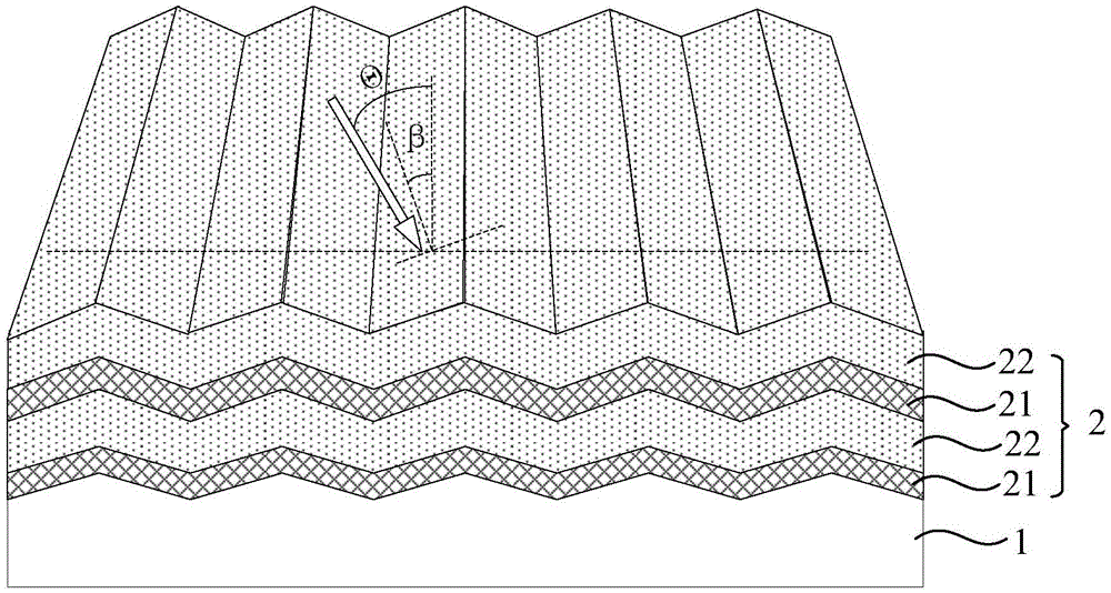
[0038] First execute step S1, please refer to the attached figure 2 , a substrate 1 is provided, and a low-energy ion beam 3 is used to irradiate the surface of the substrate 1 to form a periodic array 4 of zigzag nanostructures.
[0039] The substrate 1 is a single crystal material composed of at least two chemical elements, that is, a stoichiometric material composed of two or more chemical components. According to one embodiment, the nanofabricated material is a compound semiconductor material, in particular a III-V compound semiconductor material such as GaAs, InAs, GaSb. At the same time, the nano-fabricated material can also be a II-VI group semiconductor material, such as ZnSe, CdTe, HgS or a compound composed of two group four elements in the chemical ...
Embodiment 2
[0056] The present invention will further illustrate the preparation method of the high linear density extreme ultraviolet multilayer film blazed grating of the present invention through corresponding implementation cases and with reference to the accompanying drawings.
[0057] Step 1. Provide a GaAs substrate to be irradiated, using an energy of 1keV and a beam density of 10 15 cm -2 the s -1 , the dose is 10 19 cm -2 Ar + The ion beam irradiates the GaAs(001) surface forwardly at 410°C.
[0058] Figure 4 shows the scanning electron micrographs of the GaAs(001) surface after irradiation at 410°C, Figure 5 and Image 6 shows the transmission electron micrographs of the GaAs(001) surface after irradiation at 410°C, where, Image 6 Yes Figure 5 A magnified photograph of a single sawtooth structure in . from Figure 5 and Image 6 It can be seen that a periodic array of zigzag nanostructures is produced on the surface of GaAs, and the period of the periodic array ...
PUM
 Abstract
Description
Claims
Application Information